Pixel circuit, display device, and method of manufacturing pixel circuit

Active Publication Date: 2008-05-22
SONY CORP
View PDF3 Cites 6 Cited by
  • Summary
  • Abstract
  • Description
  • Claims
  • Application Information

AI Technical Summary

Benefits of technology

[0040]The above-described pixel circuit is a simplest circuit including the TFT 21 as driving (drive) transistor, the TFT 22 as switching transistor, and the OLED 23. However, a configuration may be employed in which switching is performed between two signals as a power signal applied to the power supply line, and switching is also performed between two signals as a video signal supplied to the signal line, thereby correcting a threshold value and mobility.
[0046]It is accordingly desirable to provide a pixel circuit, a display device, and a method of manufacturing the pixel circuit that can suppress the occurrence of shading, stripe nonuniformity and the like, and which can provide a high quality image.
[0049]According to the embodiments of the present invention, low resistance of the power supply line is achieved by forming the power supply line as multilayer wiring. A voltage drop in the wiring for power supply is thereby suppressed.
[0050]According to the embodiments of the present invention, it is possible to suppress the occurrence of shading, stripe nonuniformity and the like, and provide a high quality image.

Problems solved by technology

The former has a simple structure, but presents problems including for example a difficulty in realizing a large high-definition display.

Method used


Image

  • Pixel circuit, display device, and method of manufacturing pixel circuit
  • Pixel circuit, display device, and method of manufacturing pixel circuit
  • Pixel circuit, display device, and method of manufacturing pixel circuit

Examples


Embodiment Construction

[0073]Preferred embodiments of the present invention will hereinafter be described with reference to the drawings.

[0074]FIG. 6 is a block diagram showing a configuration of an organic EL display device using a pixel circuit according to a first embodiment of the present invention.

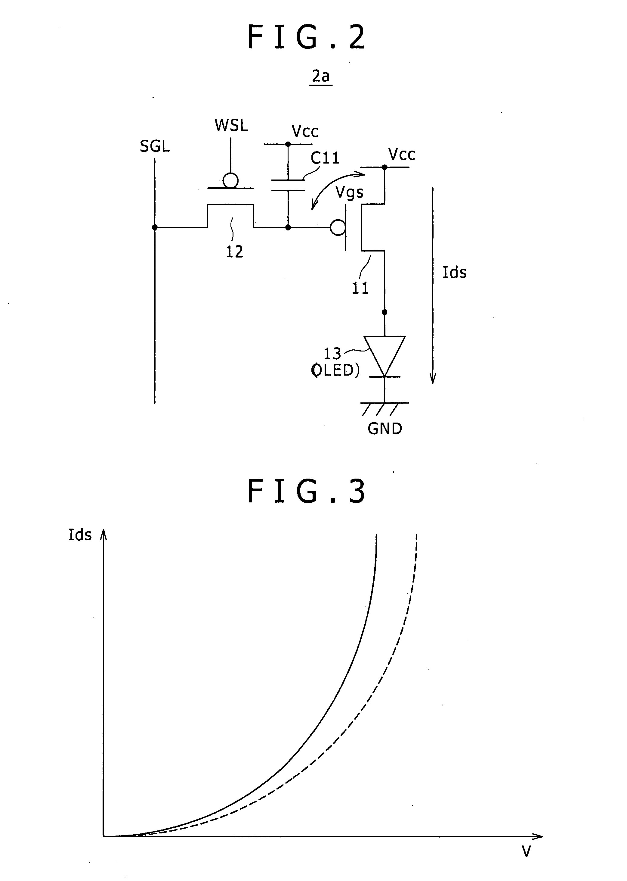
[0075]FIG. 7 is a circuit diagram showing a concrete configuration of a pixel circuit according to the first embodiment.

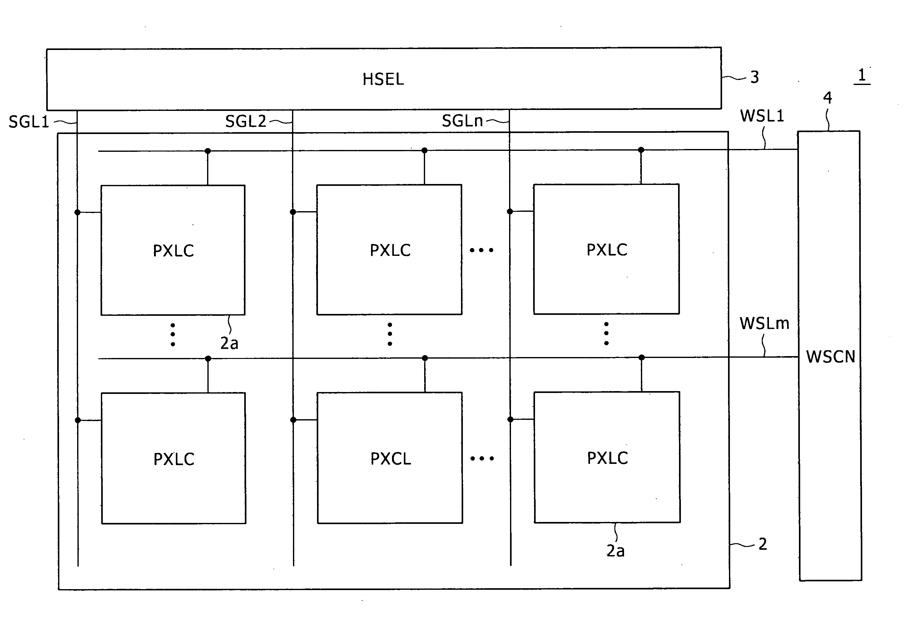
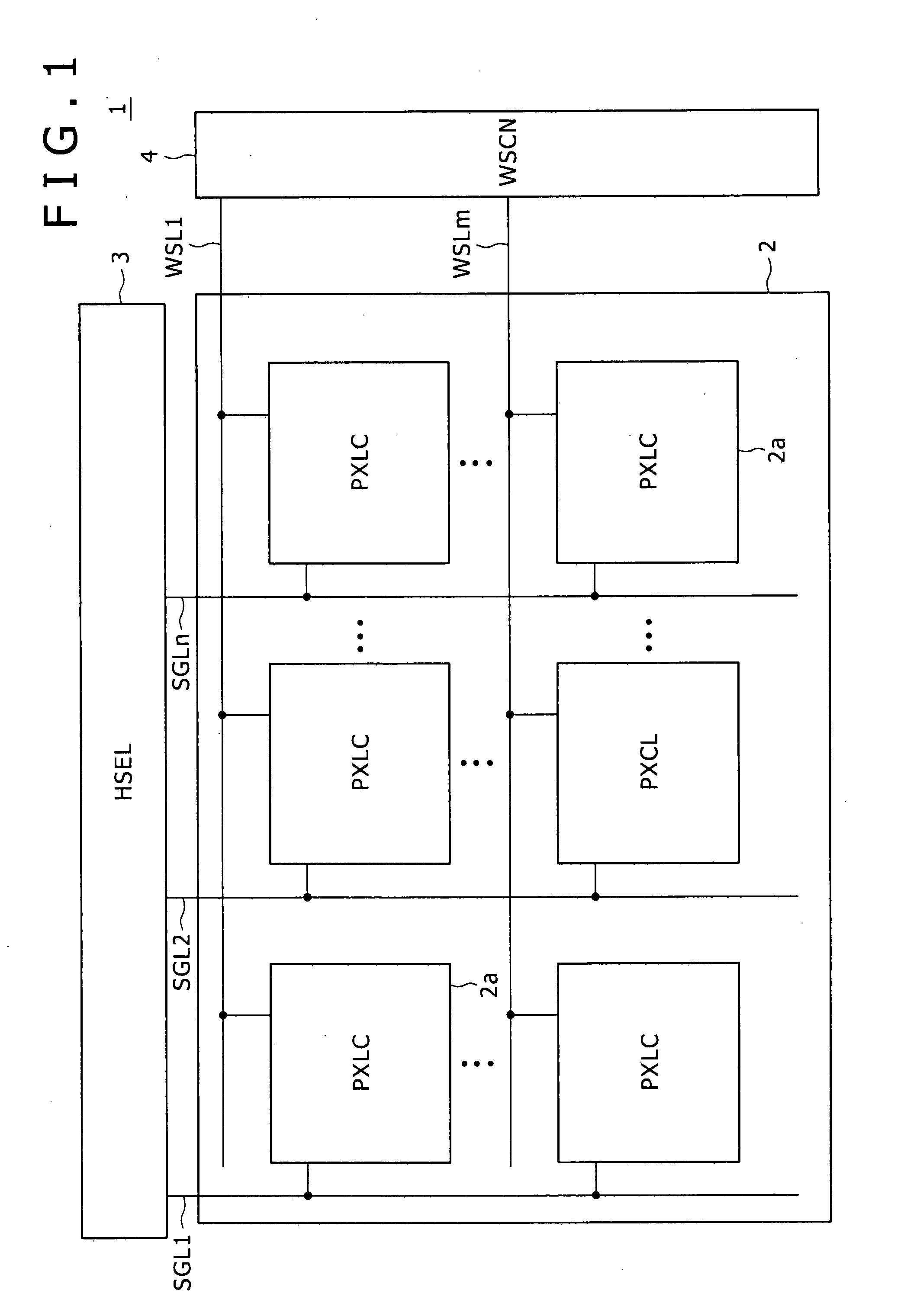
[0076]As shown in FIG. 6 and FIG. 7, this display device 100 includes: a pixel array unit 102 having pixel circuits 101 arranged in the form of an m×n matrix; a horizontal selector (HSEL) 103; a write scanner (WSCN) 104 as a second scanner; a power drive scanner (PDSCN) 105 as a first scanner; signal lines SGL101 to SGL10n selected by the horizontal selector 103 and supplied with an input signal SIN of a data signal Vsig corresponding to luminance information and an offset signal Vofs; scanning lines WSL101 to WSL10m as driving wiring selected and driven by a gate pulse (scanning pulse) GP...


PUM


Abstract

A pixel circuit including: a driving transistor; a light emitting element; and a power supply line; wherein the driving transistor is connected between the power supply line and a predetermined electrode of the light emitting element, and the power supply line is formed as multilayer wiring, and an interpolating capacitance is formed such that the power supply line formed as the multilayer wiring and another conductive layer are opposed to each other at a distance.

Description

CROSS REFERENCES TO RELATED APPLICATIONS[0001]The present invention contains subject matter related to Japanese Patent Application JP 2006-311494 filed in the Japan Patent Office on Nov. 17, 2006, the entire contents of which being incorporated herein by reference.BACKGROUND OF THE INVENTION[0002]1. Field of the Invention[0003]The present invention relates to a pixel circuit including an organic EL (Electroluminescence) light emitting element or the like, an active matrix type display device, and a method of manufacturing the pixel circuit.[0004]2. Description of the Related Art[0005]In an image display device, for example a liquid crystal display, a large number of pixels are arranged in the form of a matrix, and light intensity is controlled for each pixel according to information on an image to be displayed, whereby the image is displayed.[0006]While the same is true for an organic EL display or the like, the organic EL display is a so-called emissive display having a light emitt...

Claims


Application Information

Patent Timeline
IPC IPC(8): G09G3/30
CPCG09G3/3233G09G3/3266G09G3/3291G09G2300/0819G09G2300/0842H01L27/3276G09G2310/0256G09G2320/043G09G2320/045H01L27/3265G09G2300/0866H10K59/1216H10K59/131H05B33/22
Inventor IIDA, YUKIHITOUCHINO, KATSUHIDE
Owner SONY CORP
Why Eureka
Try Eureka