Flash Memory Device and Smart Card Including the Same

a flash memory and smart card technology, applied in static storage, digital storage, instruments, etc., can solve the problems of observable drop in current consumption, security vulnerability, and inefficiency of high voltage generator for generating high voltag

Active Publication Date: 2008-05-22
SAMSUNG ELECTRONICS CO LTD
View PDF6 Cites 9 Cited by
  • Summary
  • Abstract
  • Description
  • Claims
  • Application Information

AI Technical Summary

Benefits of technology

[0009]Exemplary embodiments of the present invention are directed to a flash memory device capable of maintaining a constant level of current consumption regardless of the number of data bits to be programmed, and a smart card including the same.

Problems solved by technology

Random access memories such as SRAM and DRAM are typically volatile memory devices.
A high voltage generator for generating high voltages is usually inefficient and an amount of current dissipated during a programming operation may depend upon the number of data bits to be programmed.
Because of this, there may be an observable drop in current consumption as memory cells are accessed.
This observable drop in current consumption may be a security vulnerability.

Method used


Image

  • Flash Memory Device and Smart Card Including the Same
  • Flash Memory Device and Smart Card Including the Same
  • Flash Memory Device and Smart Card Including the Same

Examples


Embodiment Construction

[0041]Exemplary embodiments of the present invention are described below in more detail with reference to the accompanying drawings.

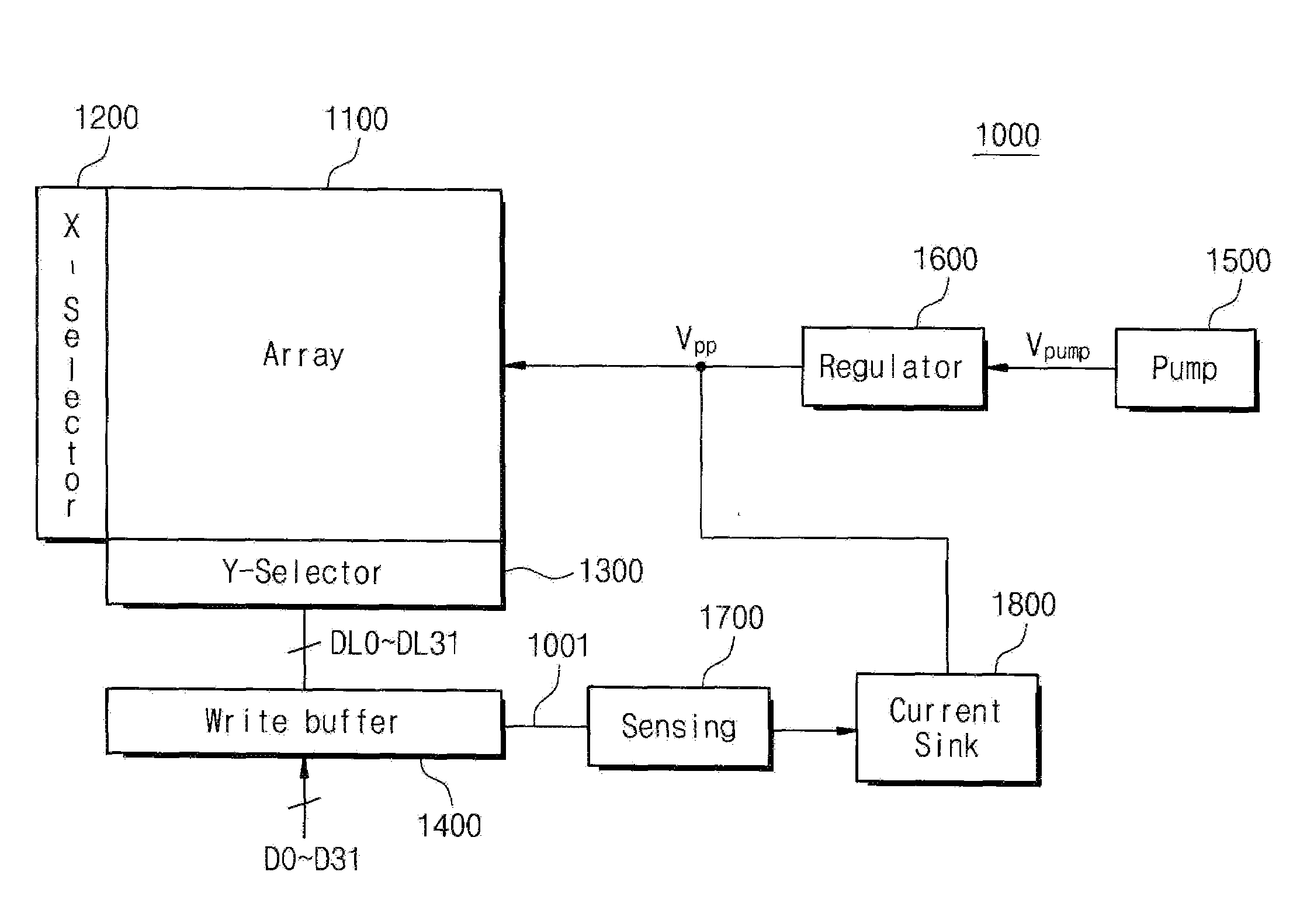
[0042]FIG. 1 is a block schematic illustrating a flash memory device in accordance with an exemplary embodiment of the present invention.

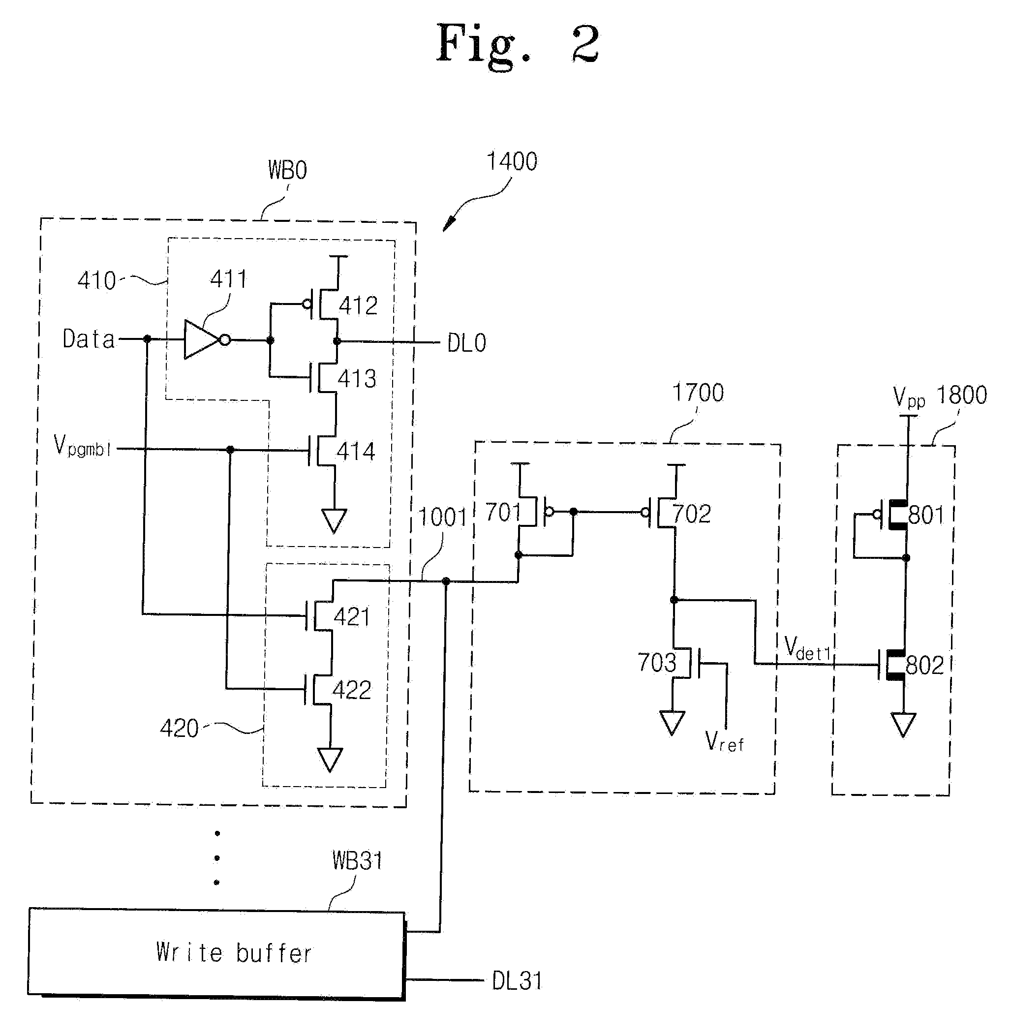
[0043]Referring to FIG. 1, the flash memory device 1000 includes a memory cell array 1100 storing N-bit data (where N is a positive integer). Although not shown, the memory cell array 1100 may be organized of memory cells arranged in rows (or word lines) and columns (or bit lines). The memory cells may be formed of, e.g., split-gate flash memory cell transistors which are erased by F-N tunneling and programmed by source-side channel hot electron injection. However, the structural configuration of the memory cells need not be limited thereto. Rows of the memory cell array 1100, for example, word lines, are selected and driven by a row selector (or X-selector) 1200. A column selector (or Y-selector) 1300 operates to sele...


PUM


Abstract

A flash memory device includes an array having memory cells arranged in rows and columns. A high voltage generator is configured to supply a high voltage to the array during a programming operation. Write buffers corresponding to selected memory cells drive the selected memory cells with a program voltage or a program-inhibition voltage in response to input data. Each write buffer consumes a dummy cell current when input data is program-inhibited data. A current-voltage conversion circuit connected to the write buffers through a common sensing line supplies a current to the write buffers as the dummy cell current through the common sensing line and outputs a voltage proportional to the current, supplied to the write buffers. A current sink circuit discharges a current from an output of the high voltage generator in response to a voltage output from the current-voltage conversion circuit.

Description

CROSS-REFERENCE TO RELATED APPLICATION[0001]This application claims priority under 35 U.S.C, 119 to Korean Patent Application No. 10-2006-0115392, filed on Nov. 21, 2006, the entire contents of which are hereby incorporated by reference.BACKGROUND OF THE INVENTION[0002]1. Technical Field[0003]The present disclosure relates to flash memory, and more particularly, to a flash memory device and a smart card including the same.[0004]2. Discussion of the Related Art[0005]Semiconductor memory devices are generally classified as volatile or nonvolatile according to whether memory can be retained in the absence of power. Random access memories such as SRAM and DRAM are typically volatile memory devices. Nonvolatile memory devices include read-only memories (ROMs), e.g., erasable and programmable ROMs (EPROMs), electrically erasable and programmable ROMs (EEPROMs), and flash memories.[0006]Modern flash memory devices have small size, low power consumption, and advanced reading / writing perform...

Claims


Application Information

Patent Timeline
Patent Type & Authority Applications(United States)
IPC IPC(8): G11C16/06
CPCG11C5/147G11C16/30G11C16/22
Inventor LEE, BYEONG-HOON
Owner SAMSUNG ELECTRONICS CO LTD
Why Eureka
Try Eureka