Contamination reducing liner for inductively coupled chamber

Inactive Publication Date: 2008-05-22
APPLIED MATERIALS INC
View PDF40 Cites 52 Cited by
  • Summary
  • Abstract
  • Description
  • Claims
  • Application Information

AI Technical Summary

Benefits of technology

[0010]In yet another embodiment, a method for depositing a film on a substrate by plasma enhance chemical vapor deposition may include disposing a substrate in a processing chamber having a coil extending around a substrate support assembly, wherein the coil is separated from the substrate support by a quartz liner protected by a first

Problems solved by technology

However, during plasma enhanced deposition processes, sputtering of chamber components may contaminate or otherwise result in poor quality of the deposited silicon film, thereby contributing to poor performance of the circuit or device.

Method used


Image

  • Contamination reducing liner for inductively coupled chamber
  • Contamination reducing liner for inductively coupled chamber
  • Contamination reducing liner for inductively coupled chamber

Examples


Embodiment Construction

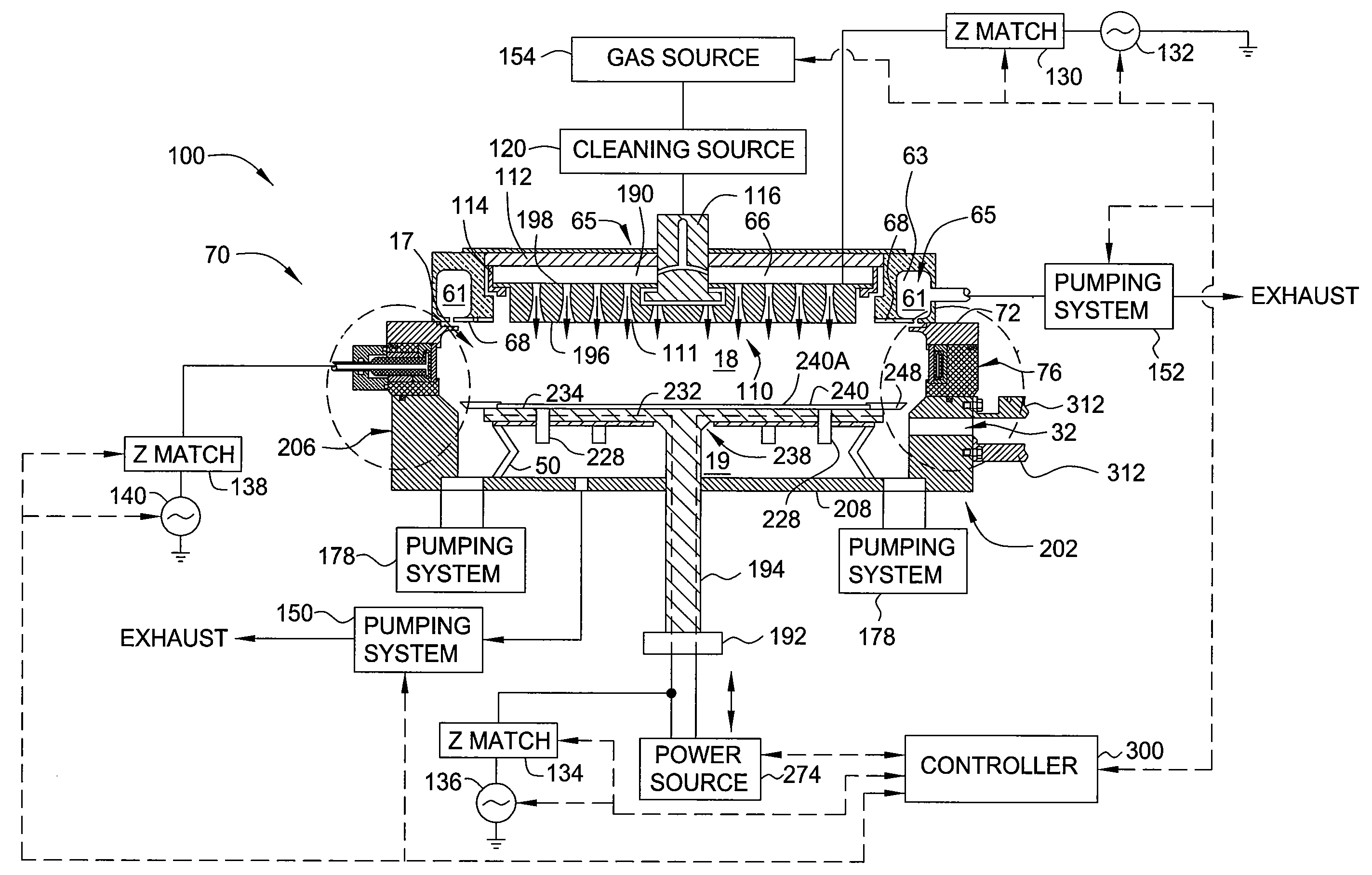
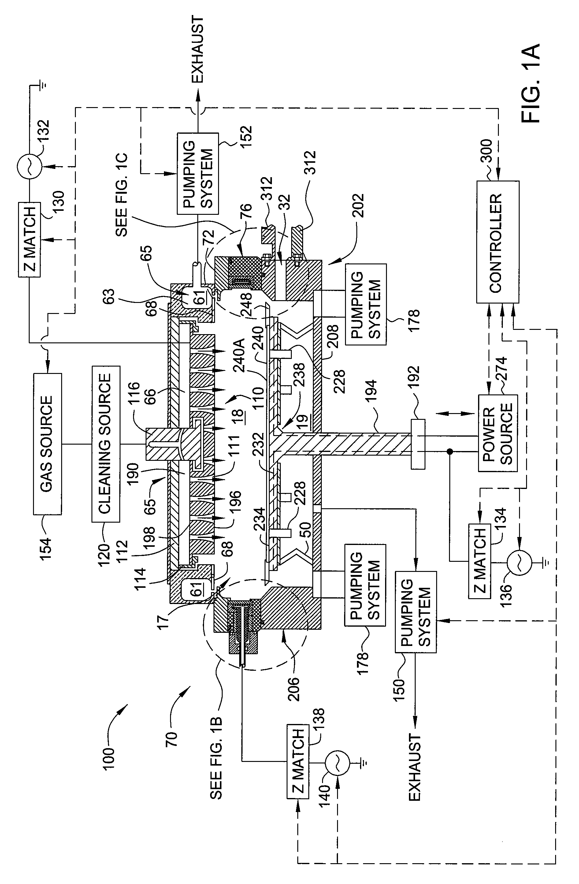
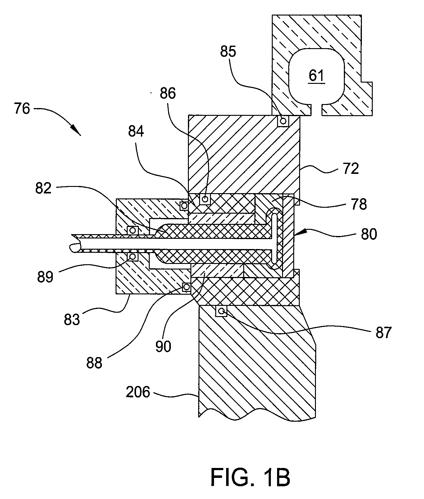
[0018]Various embodiments of the invention are generally directed to an apparatus and method for reducing contamination in a processing chamber using an inductively coupled high density plasma. In general, various aspects of the present invention may be used for flat panel display processing, semiconductor processing, solar cell processing, or other substrate processing. The processing chamber includes a coil disposed in the chamber and routed proximate the chamber wall. A ceramic liner is disposed over the coil and is protected by a coating of a material, wherein the coating of material has a film property similar to the ceramic liner. Additionally, the coating of material also has a similar film property to a deposition film deposited on a substrate. Thus, in the event that some of the protective coating of material is inadvertently sputtered during plasma processing, the sputtered material will not become a source of contamination if deposited on the substrate along with the depo...


PUM

PropertyMeasurementUnit
Thicknessaaaaaaaaaa
Poweraaaaaaaaaa

Abstract

A method and apparatus for depositing a film through a plasma enhance chemical vapor deposition process is provided. In one embodiment, an apparatus includes a processing chamber having a coil disposed in the chamber and routed proximate the chamber wall. A liner is disposed over the coil and is protected by a coating of a material, wherein the coating of material has a film property similar to the liner. In one embodiment, the liner is a silicon containing material and is protected by the coating of the material. Thus, in the event that some of the protective coating of material is inadvertently sputtered, the sputter material is not a source of contamination if deposited on the substrate along with the deposited deposition film on the substrate.

Description

CROSS-REFERENCE TO OTHER APPLICATIONS[0001]This application claims the benefit of U.S. Provisional Patent Application Ser. No. 60 / 829,279, filed Oct. 12, 2006, (Attorney Docket No. APPM / 11572L) which is herein incorporated by reference.BACKGROUND OF THE INVENTION[0002]1. Field of the Invention[0003]Embodiments of the present invention generally relate to substrate processing apparatuses and methods, such as apparatuses and methods for flat panel display processing apparatuses (i.e. LCD, OLED, and other types of flat panel displays), semiconductor wafer processing, solar panel processing, and the like.[0004]2. Description of the Related Art[0005]Plasma enhanced chemical vapor deposition (PECVD) is generally employed to deposit thin films on a substrate such as a silicon or quartz wafer, large area glass or polymer workpiece, and the like. Plasma enhanced chemical vapor deposition is generally performed by introducing a precursor gas into a vacuum chamber that contains the substrate. ...

Claims


Application Information

Patent Timeline
IPC IPC(8): C23C16/00
CPCC23C16/4404
Inventor CHOI, SOO YOUNGWANG, QUNHUA
Owner APPLIED MATERIALS INC
Why Eureka
Try Eureka