Memory device and semiconductor device

Inactive Publication Date: 2008-05-29
SEMICON ENERGY LAB CO LTD
View PDF9 Cites 20 Cited by
  • Summary
  • Abstract
  • Description
  • Claims
  • Application Information

AI Technical Summary

Benefits of technology

[0008]In view of the foregoing problem, it is an object of the present invention to provide a flexible memory device and a flexible semiconductor device with a highly reliable storage function in which the element having a layer containing an organic compound is provided.
[0015]The memory device and the semiconductor device of the present invention include the memory element having a layer including an organic compound between a pair of electrodes formed of the first electrode layer and the second electrode layer, the element layer having the memory element, and the sealing layer formed over the element layer, and the moisture absorbing material is contained in the sealing layer. The moisture absorbing material is contained in the sealing layer, whereby, if water in an atmosphere to which the memory device or the semiconductor device is exposed enters the sealing layer, the moisture absorbing material contained in the sealing layer can absorb the water. Therefore, contact of water with the memory element which has a layer including an organic compound between a pair of electrodes formed of the first electrode layer and the second electrode layer can be suppressed.
[0016]As a result, deterioration of layers including the first electrode, the second electrode, and the organic compound, or the like, which is caused by water or vapor can be suppressed. Further, variation with time in the memory storage characteristic of the memory element can be suppressed, and a memory device and a semiconductor device with a highly reliable storage function can be manufactured. Furthermore, the element layer and the sealing layer are provided over a flexible substrate, whereby a memory device and a semiconductor device with high reliability in retention for storing data, which are extremely thin and flexible, can be manufactured.

Problems solved by technology

However, unfortunately, the memory element which has a layer containing an organic compound is readily damaged as shown in the Patent Document 1, depending on usage environments.
As a result, undesirable reduction of reliability in storage function of the memory device and the semiconductor device, specifically, a writing characteristic, a reading characteristic, a memory storage characteristic, or the like frequently takes place.

Method used


Image

  • Memory device and semiconductor device
  • Memory device and semiconductor device
  • Memory device and semiconductor device

Examples


embodiment mode 1

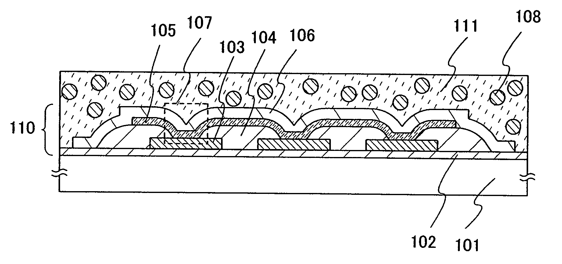
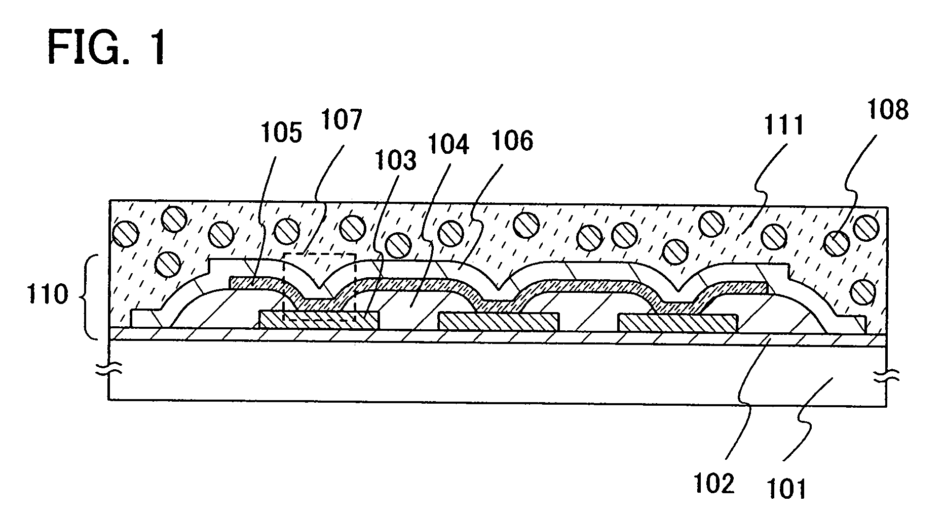
[0035]In this embodiment mode, a main structure of a memory device of the present invention will be described. Typically, a memory device having a memory cell in which a memory element is provided will be explained with reference to FIG. 1, FIGS. 2A to 2C and FIGS. 4A to 4C. Note that each memory element has a layer including an organic compound between a pair of electrodes formed of a first electrode layer and a second electrode layer, and the memory cell are arrange in matrix in the memory device. Also, a structure of the memory element will be explained with reference to FIGS. 3A to 3F.

[0036]As shown in FIG. 4A, a memory device 127 has a memory cell array 132 and a driving circuit to drive the memory cell array. In the memory cell array 132, the memory cells 21 are provided in matrix. The memory cell 21 has a memory element 107 (see FIG. 1). The memory element 107 has the first electrode layer 103 extending in a first direction, a layer 105 including an organic compound which cov...

embodiment mode 2

[0119]In this embodiment mode, in the memory device shown in the above embodiment mode, a main structure of a memory device having a memory cell array where memory cells each have a switching element and a memory element will be explained using FIG. 5 and FIGS. 6A to 6C. FIG. 5 is a cross sectional view of the memory device in this embodiment mode, and FIGS. 6A to 6C illustrate a structure of the memory device in this embodiment mode.

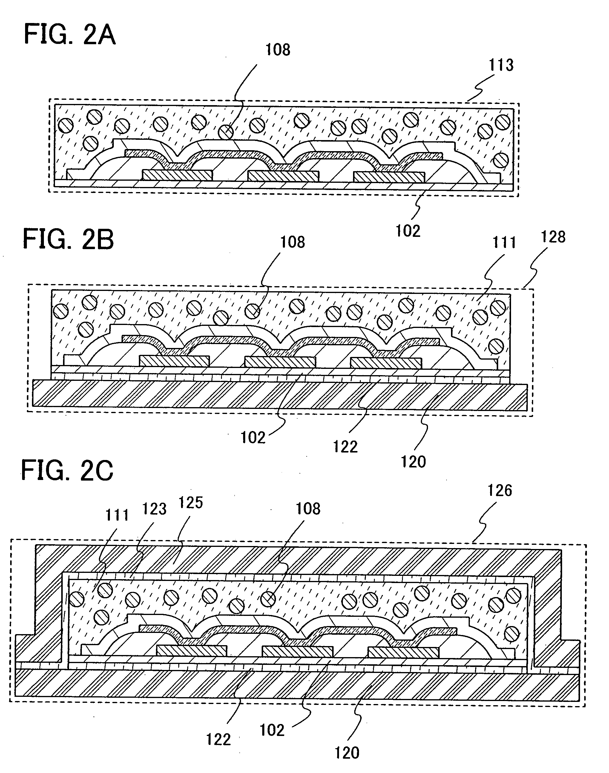
[0120]Note that the mode shown in FIG. 5 is a deformed example of the mode shown in FIG. 2C, and a mode where the element layer and the sealing layer are sealed with the flexible substrate is shown. In the mode shown in FIG. 5, the switching element and the memory element is formed in the element layer of the memory device shown in FIG. 1, FIGS. 2A and 2B.

[0121]As shown in FIG. 6A, a memory device 221 in this embodiment mode has a memory cell array 222 and a driver circuit which drives the memory cell array 222. The memory cell array 222 has a plurality...

embodiment mode 3

[0142]In this embodiment mode, one mode of a semiconductor device which is formed by the peeling method shown in the above embodiment mode will be described below. Typically, a main structure of a semiconductor device which can perform transmission / reception of instructions or data with radio signals will be explained with reference to FIG. 7 and FIG. 8. FIG. 7 is a cross sectional view of the semiconductor device in this embodiment mode. FIG. 8 illustrates a structure of the semiconductor device in this embodiment mode. Note that the semiconductor device in this embodiment mode has a memory portion including the memory cell array shown in the above embodiment mode.

[0143]FIG. 8 is a block diagram illustrating a structural example of the semiconductor device which can perform transmission / reception of instructions or data with radio signals. Such a semiconductor device includes an antenna 312, an RF circuit portion 313, a power supply circuit portion 315, and a logic circuit portion ...


PUM


Abstract

It is an object to provide a flexible semiconductor device bearing a memory device with a highly reliable storage function, where the memory device comprises a layer containing an organic compound. Specifically, the memory device has a memory element which comprises a layer including an organic compound between a pair of electrodes and a sealing layer formed over the memory element, and a moisture absorbing material is contained in the sealing layer. As the moisture absorbing material, a particle of molten silica, crystalline silica, alumina, silicon nitride, aluminum nitride, boron nitride, zeolite, an oxide of an alkaline earth metal, sulfate or a high water-absorbing polymer can be used.

Description

BACKGROUND OF THE INVENTION[0001]1. Field of the Invention[0002]The present invention relates to a memory device and a semiconductor device bearing a memory element which has a layer including an organic compound.[0003]2. Description of the Related Art[0004]In recent years, an organic thin film transistor, a memory element, and the like, which include an organic compound, for a control circuit, a memory circuit, and the like have been intensively developed (for example, see Patent Document 1: Japanese Published Patent Application No. 2006-148080).[0005]Further, a semiconductor device having various functions, in which a plurality of circuits is integrated on an insulating surface, has been developed. Furthermore, a semiconductor device which can transmit and receive data wirelessly by providing an antenna has been developed. Such a semiconductor device is referred to as a wireless chip (also referred to as an ID tag, an IC tag, an IC chip, an RF (Radio Frequency) tag, a wireless tag...

Claims


Application Information

Patent Timeline
IPC IPC(8): G06K19/06H01L51/10H01L51/40
CPCB82Y10/00G11C13/0014H01L27/285H01L51/107H01L51/0595H01L51/10H01L51/0591H10K19/202H10K10/80H10K10/50H10K10/88H10K10/701H10K19/00H10K10/00
Inventor NOMURA, RYOJI
Owner SEMICON ENERGY LAB CO LTD
Why Eureka
Try Eureka