Avalanche photodiode detector

a photodiode detector and photodiode technology, applied in the field of photodiode detectors, can solve the problems of reducing the overall quantum efficiency and after pulsing performance of an apd, affecting the selection of materials, and affecting the quality of the photodiod

Inactive Publication Date: 2008-05-29
THE BOEING CO
View PDF2 Cites 36 Cited by
  • Summary
  • Abstract
  • Description
  • Claims
  • Application Information

AI Technical Summary

Problems solved by technology

This may lead to some interface defects.
Due to interface defects there may be some carrier traps and recombination centers, which reduce overall quantum efficiency and after puls

Method used


Image

  • Avalanche photodiode detector
  • Avalanche photodiode detector
  • Avalanche photodiode detector

Examples


Embodiment Construction

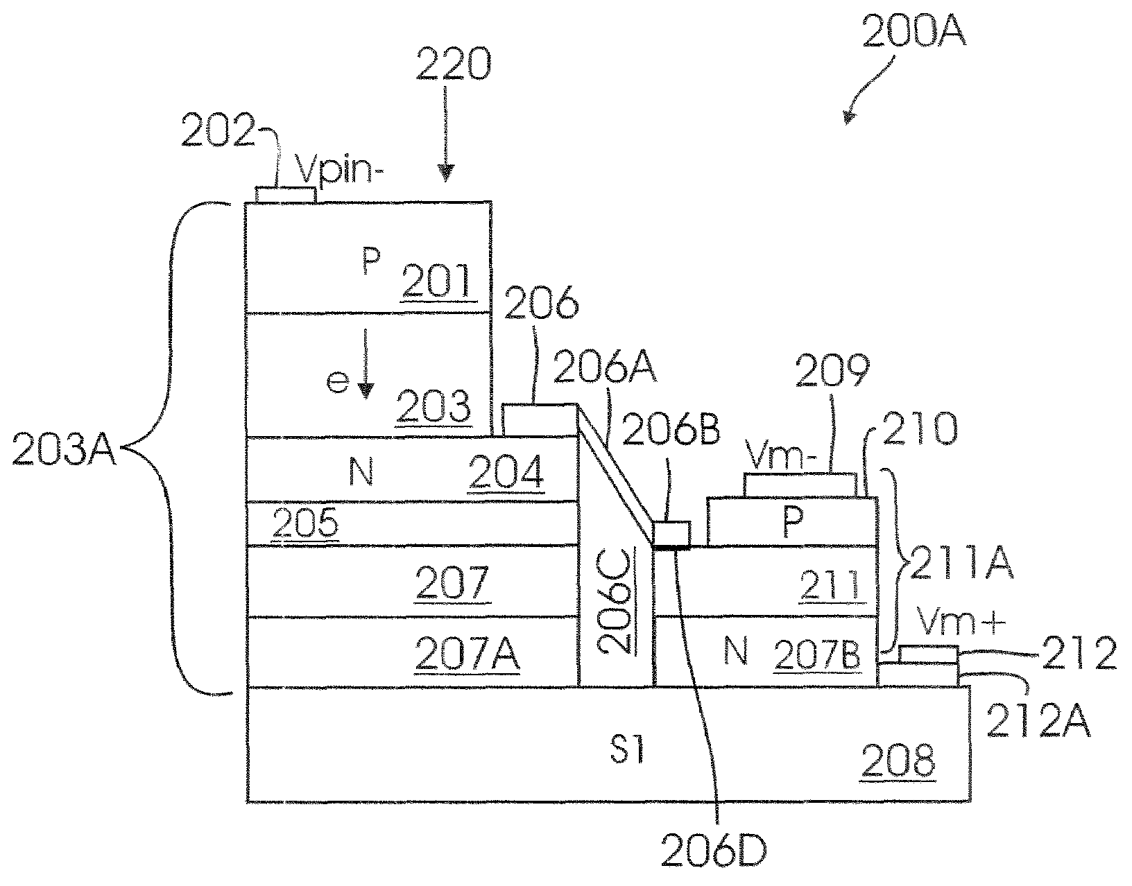
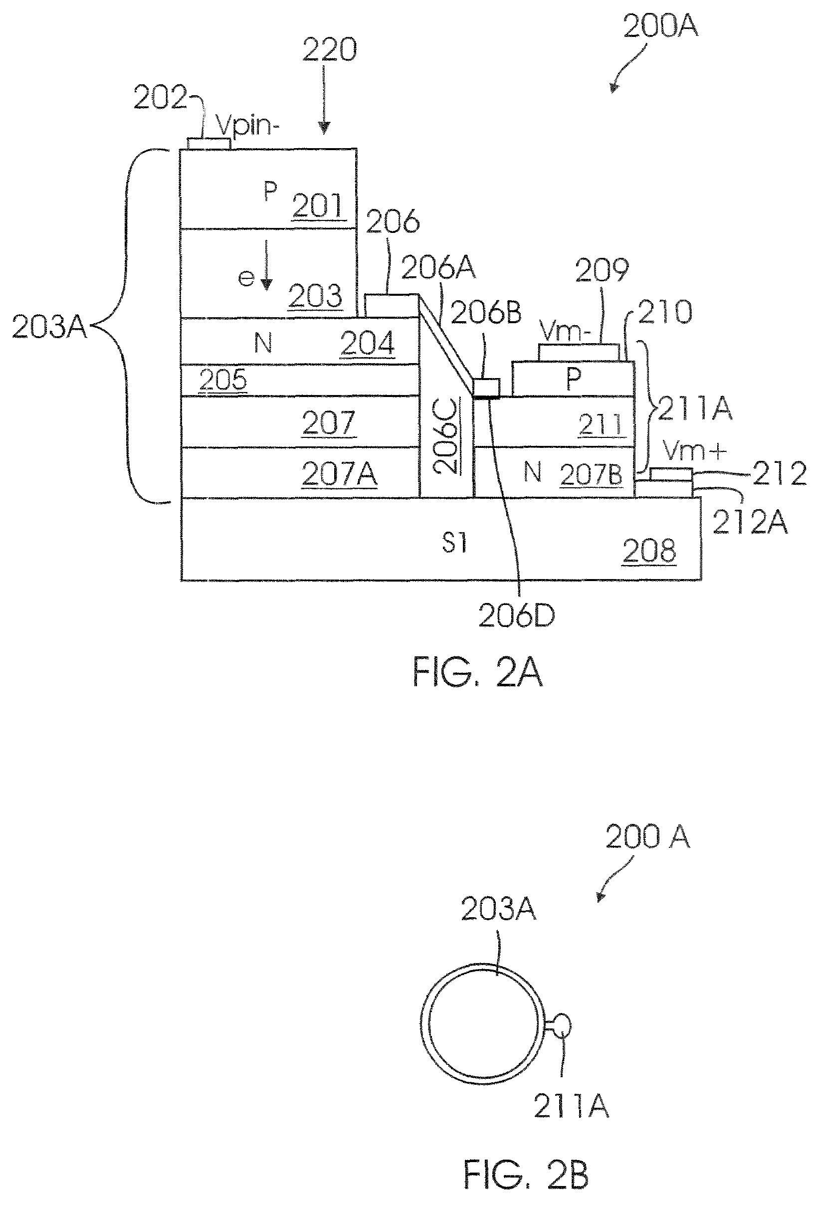
[0018]In one aspect of the present invention, a three terminal APD structure with separate absorption and multiplication layer (also referred to as “TT-SAM APD or APD”) is provided. The absorption layer and multiplication layer may be grown separately and hence are controlled independently. This allows one to select different materials for the absorption and multiplication layer. The APD of the present invention also provides an additional terminal. The additional terminal enables individual control of bias across an absorption (Absorber”) region and a multiplication (“Multiplier”) region.

[0019]To facilitate an understanding of APD structure, a general overview of a conventional APD structure will be described. The specific structural components and layers of APD of the present invention, will then be described with reference to general structure of APD.

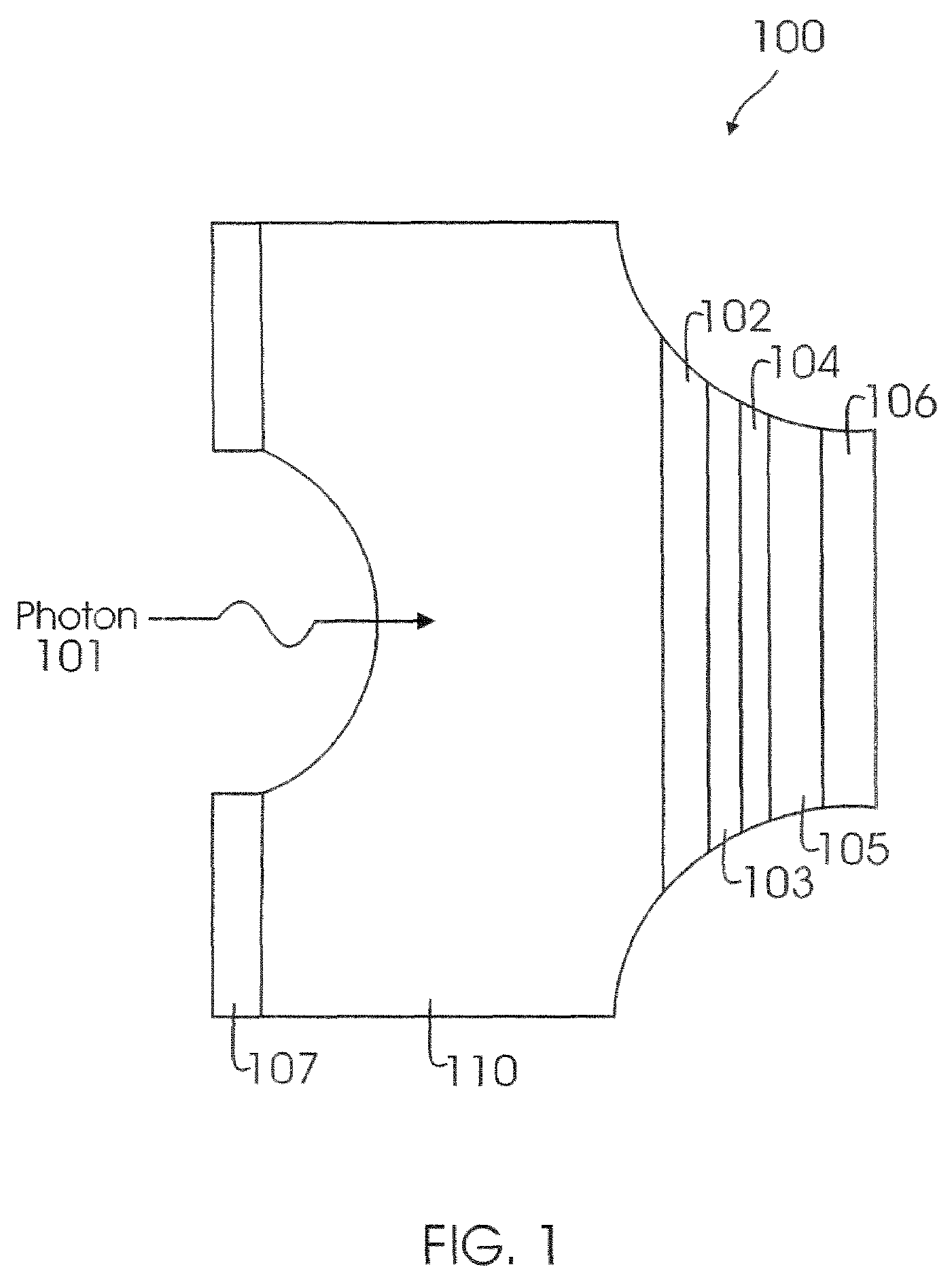
[0020]FIG. 1 shows a top level block diagram of a conventional APD structure. APD 100 includes a P-InP substrate layer 110; a P-InP...


PUM


Abstract

An avalanche photodiode detector is provided. The avalanche photodiode detector comprises an absorber region having an absorption layer for receiving incident photons and generating charged carriers; and a multiplier region having a multiplication layer; wherein the multiplier region is on a mesa structure separate from the absorber region and is coupled to the absorber region by a bridge for transferring charged carriers between the absorber region and multiplier region.

Description

1. FIELD OF THE INVENTION[0001]The present invention relates generally to photodiode detectors, and more particularly to avalanche photodiode detectors.2. BACKGROUND[0002]Avalanche photodiode detectors (APDs) are photosensitive devices that detect optical power by converting an input signal (photons) to an electrical signal. The input signal is amplified by an “avalanche effect” when carriers are infected in an area with high electrical field. This occurs because multiple electron-hole pairs are created for each absorbed photon.[0003]An APD typically comprises of a plurality of stacked layers including a multiplication layer and an absorption layer on a semiconductor substrate. The absorption layer absorbs incident photons to create electron / holes that are transferred to the multiplication layer. The multiplication layer multiplies the electrons / holes. This occurs when electron / holes have sufficient energy to create a new electron and hole. Initial carriers and newly created carrier...

Claims


Application Information

Patent Timeline
IPC IPC(8): H01L31/102
CPCB82Y20/00H01L31/1075H01L31/035236H01L31/035281H01L31/108Y02E10/50
Inventor YUAN, PINGBOISVERT, JOSEPH C.KRUT, DMITRI D.SUDHARSANAN, RENGARAJAN
Owner THE BOEING CO
Why Eureka
Try Eureka