Nonvolatile semiconductor memory
- Summary
- Abstract
- Description
- Claims
- Application Information
AI Technical Summary
Benefits of technology
Problems solved by technology
Method used
Image

Examples
first embodiment
(1) First Embodiment
[0041](a) Structure
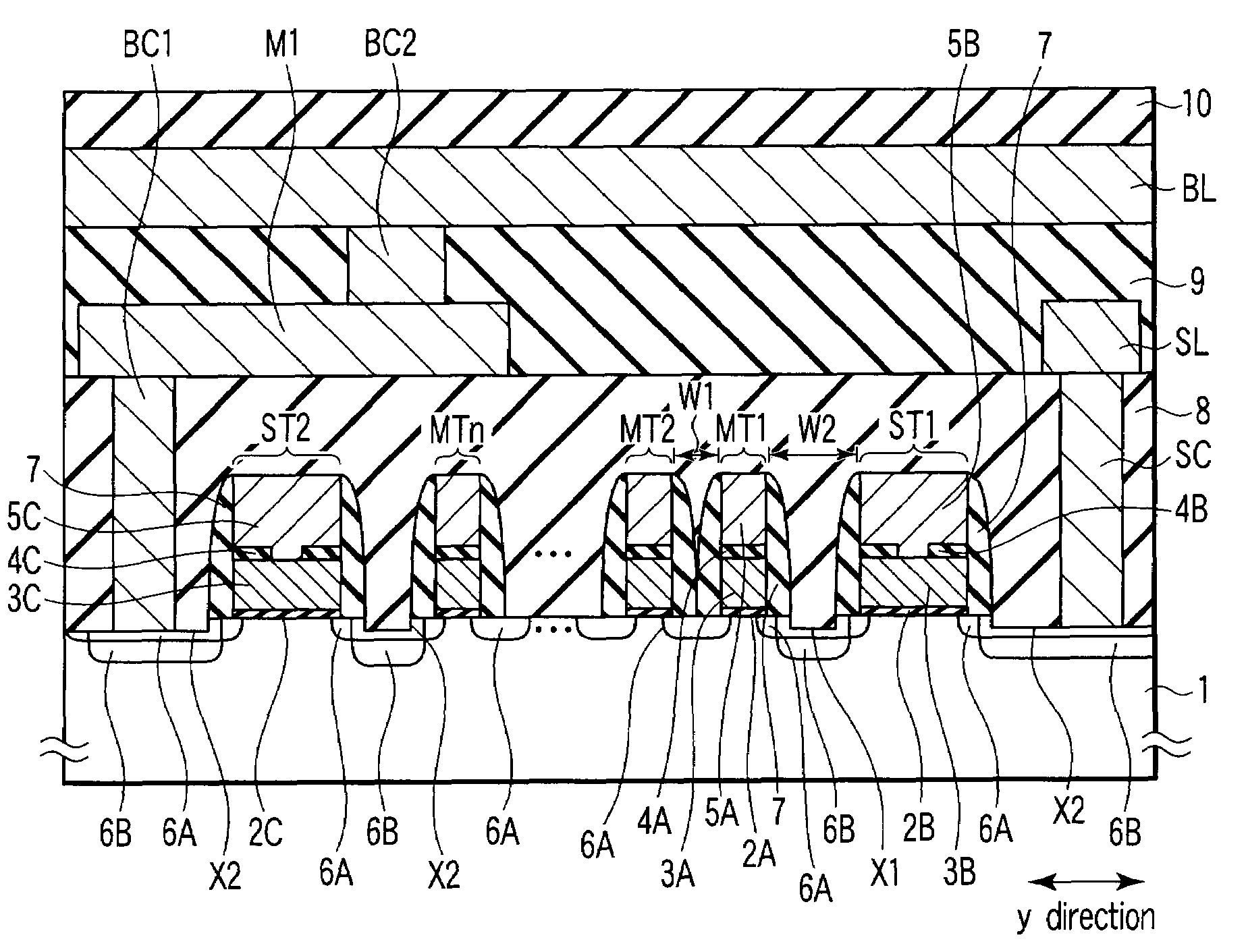
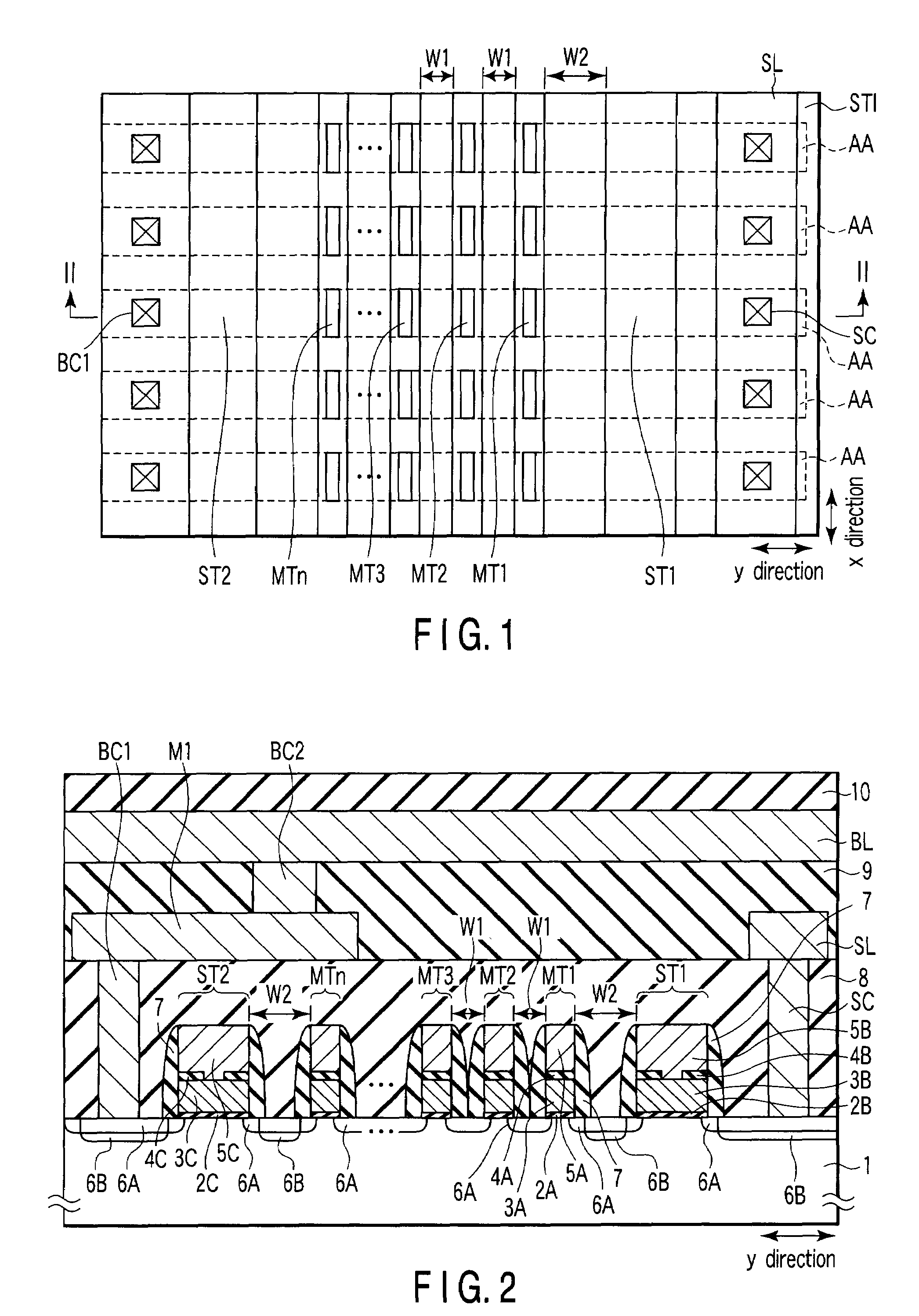
[0042]The structure of a nonvolatile semiconductor memory embodying the invention will be described with reference to FIGS. 1 and 2. This embodiment will be described in terms of a flash memory, which is an example of the nonvolatile semiconductor memory.
[0043]FIG. 1 is a plan view of the flash memory of the embodiment. FIG. 2 is a sectional view taken along line II-II of FIG. 1 in the y direction. The flash memory illustrated in FIGS. 1 and 2 is a NAND type flash memory.
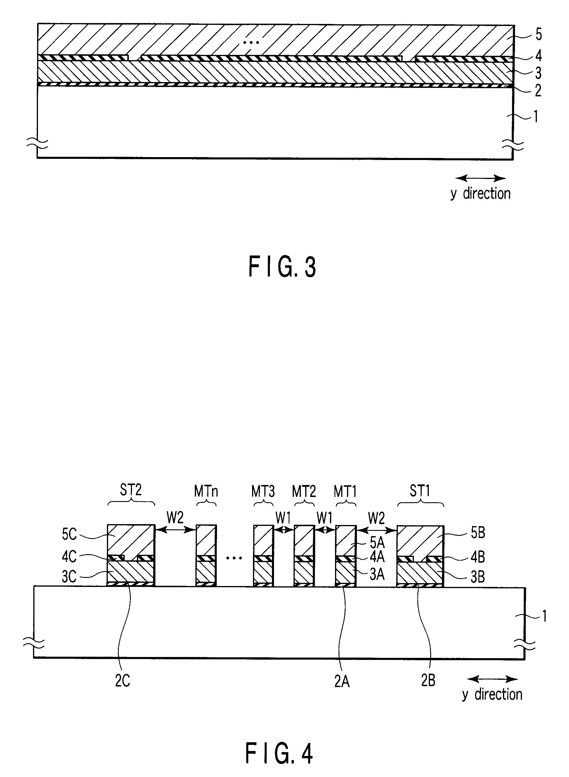
[0044]The surface region of a semiconductor substrate 1 is composed of isolation insulating regions STI of, for example, a shallow trench isolation (STI) structure and active regions (device regions) AA surrounded by the isolation insulating regions. The active regions AA, which are shown enclosed by dashed lines in FIG. 1, extend along the y direction (first direction) in FIG. 1.
[0045]A number of memory cell transistors MT1 to MTn (n is a natural number) is arranged in each of...
first modification
(1) First Modification
[0094](a) Structure
[0095]Reference is made to FIGS. 11 and 12 to describe the structure of a flash memory according to this modification. FIG. 11 is a plan view of this flash memory. FIG. 12 is a sectional view taken along line II-II of FIG. 11 in the y direction. In FIGS. 11 and 12, like reference numbers are used to denote corresponding parts to those in FIGS. 1 and 2, thereby simplifying the description.
[0096]In this modification, the gate spacing W3 of two adjacent transistors of the memory cell transistors MT2 to MTn-1 is set such that W132. That is, the memory cell transistors MT1 and MTn are displaced to the sides of the memory cell transistors MT2 and MTn-1, respectively, to thereby increase the spacings between the transistors ST1 and MT1 and between the transistors ST2 and MTn. Thus, the relation such that W132 holds.
[0097]In addition, if the spacings between the transistors ST1 and MT1 and between the transistors ST2 and MTn prior to displacement of ...
second modification
(2) Second Modification
[0104](a) Structure
[0105]The structure of a flash memory according to this modification will be described with reference to FIG. 14, in which like reference numbers are used to denote corresponding parts to those in FIG. 2, thereby simplifying the description.
[0106]This modification has the features of the first embodiment and is additionally characterized in that a recess X1 is formed in the source diffusion layers 6A and 6B of the memory cell transistor MT1 which are shared with the select gate transistor ST1. In this case, recesses X2 are also formed in the source diffusion layers 6A and 6B of the select gate transistor ST1 and the source and drain diffusion layers 6A and 6B of the select gate transistor ST2.
[0107]Thereby, GIDL-based hot electrons make a detour to avoid the recess X1 and move in the diffusion layers 6A and 6B toward the memory cell transistor MT1.
[0108]Therefore, the distance moved by the hot electrons becomes longer than W2, further increa...
PUM
 Abstract
Description
Claims
Application Information
 - Generate Ideas
- Intellectual Property
- Life Sciences
- Materials
- Tech Scout
- Unparalleled Data Quality
- Higher Quality Content
- 60% Fewer Hallucinations
Browse by: Latest US Patents, China's latest patents, Technical Efficacy Thesaurus, Application Domain, Technology Topic, Popular Technical Reports.
© 2025 PatSnap. All rights reserved.Legal|Privacy policy|Modern Slavery Act Transparency Statement|Sitemap|About US| Contact US: help@patsnap.com