
Collective and synergistic MRAM shields

a technology of mram shields and shields, applied in the field of collective and synergistic mram shields, can solve the problems of data stored therein being susceptible to being corrupted or destroyed, and corrupting the memory therein,

Active Publication Date: 2008-05-29
TESSERA INC
View PDF35 Cites 45 Cited by
  • Summary
  • Abstract
  • Description
  • Claims
  • Application Information

AI Technical Summary

Benefits of technology

[0005]The tunnel magnetoresistance effect (“TMR”) causes the resistance of the insulator between the plates to change depending on the state of the cell. Generally, the resistance of the insulator is higher when the polarity of the plates is different (or “antiparallel”) than when the plates have the same polarity (parallel). This effect is used in reading data from the memory.
[0011]In accordance with still another embodiment of the invention, a microelectronic assembly can include a substrate extending in first and second transverse directions defining a plane and a magnetic field sensor. At least one MRAM die may be conductively connected to the substrate. A first electromagnetic coil can be oriented in the first direction. A second electromagnetic coil can be oriented in the second direction. Control circuitry may be in electronic communication with the magnetic field sensor, the first electromagnetic coil and the second electromagnetic coil. The control circuitry can be operable in response to output representing a magnetic field sensed by the magnetic field sensor and can control the first and second electromagnetic coils to generate an opposite magnetic field for neutralizing the sensed magnetic field.

Problems solved by technology

Due to the nature of the MRAM structure, the data stored therein is susceptible to being corrupted or destroyed by stray magnetic fields.
Essentially, a stray magnetic field which encounters the memory array can change the polarity of one or more cells, thereby corrupting the memory therein.

Method used


Image

  • Collective and synergistic MRAM shields
  • Collective and synergistic MRAM shields
  • Collective and synergistic MRAM shields

Examples


Embodiment Construction

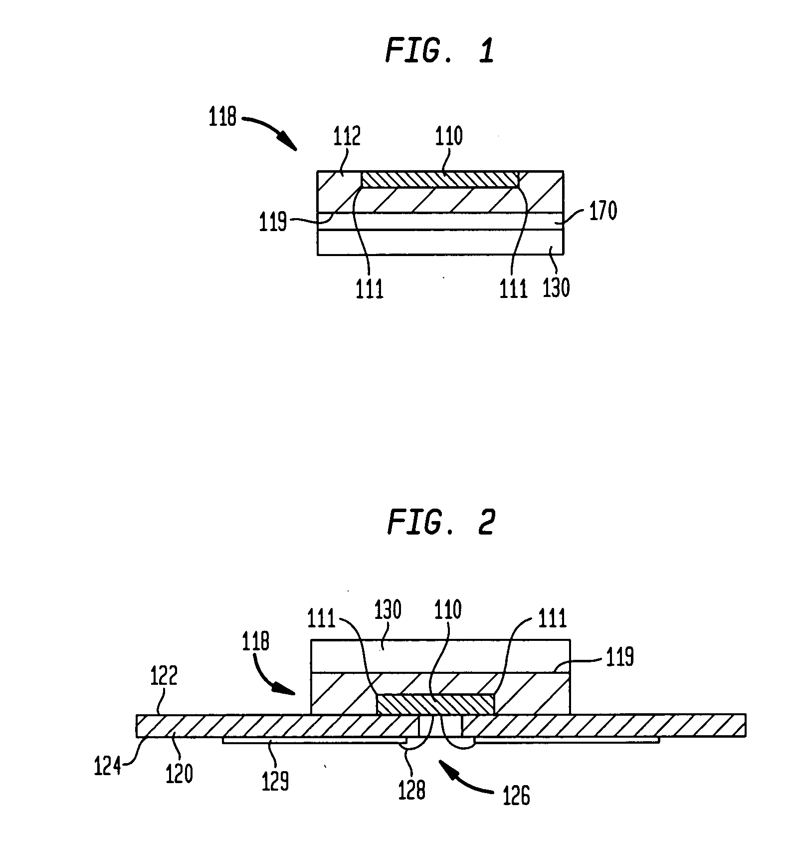
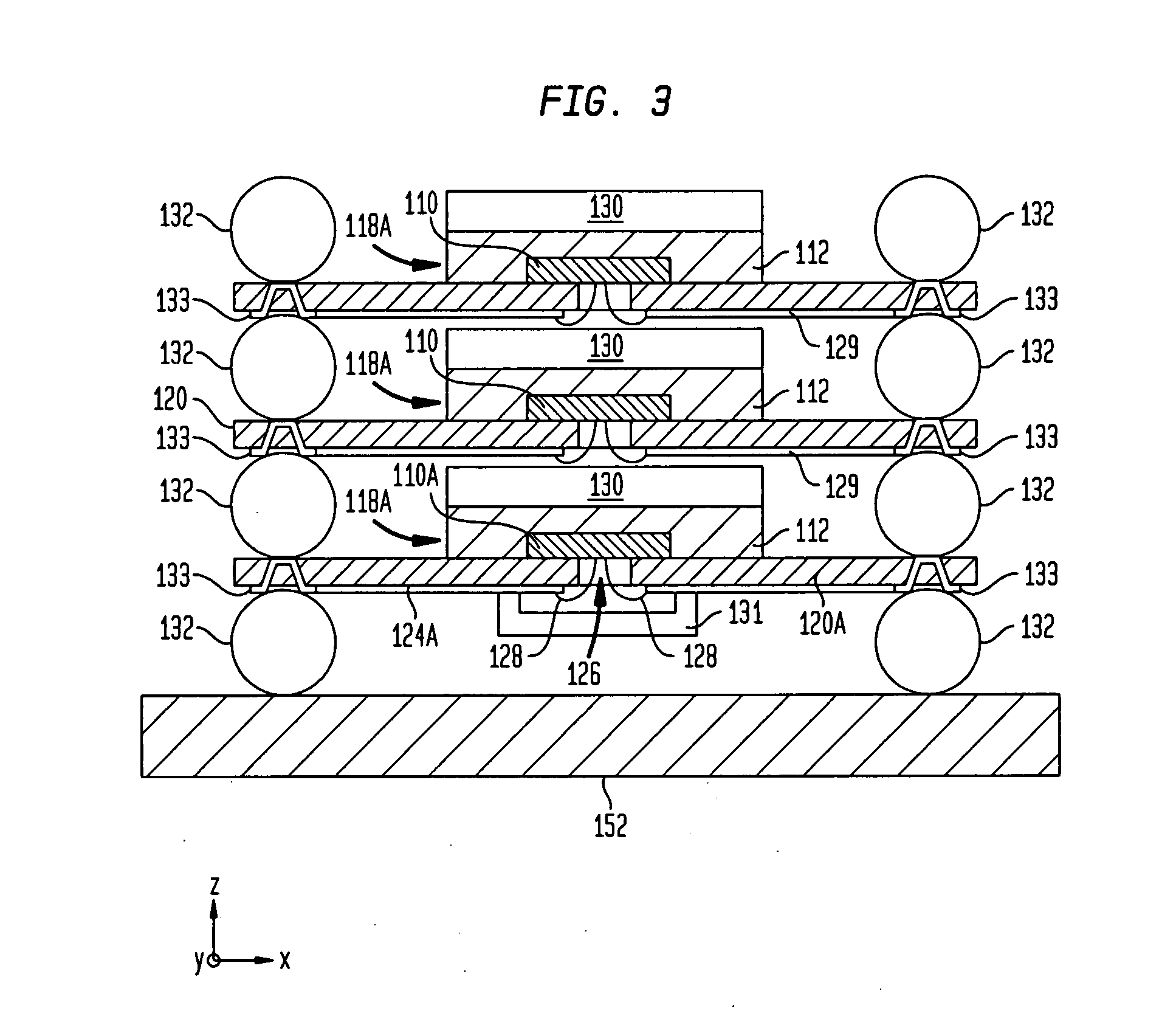
[0032]Referring now to the drawings, wherein like reference numerals indicate like elements, FIG. 1 shows an MRAM die 118 including MRAM circuitry 110 within dielectric 112. As shown in FIG. 2, MRAM die 118 may be mounted to a substrate 120 which made from a dielectric material and is generally planar having a first surface 122 and a second, opposite surface 124. MRAM die 118 can be mounted to substrate 120 using known methods for flip-chip bonding such that die 118, particularly MRAM circuitry 110 within die 118 is electronically interconnected with conductive elements 129 exposed at a surface of substrate 120. In the embodiment shown in FIGS. 2 and 3, hole 126 is formed within substrate 120 through which wires 128 pass. Wires 128 interconnect MRAM circuitry 110 with the conductive elements 129 of substrate 120.

[0033]Generally, materials having one of two different properties are useful to divert magnetic fields. One such material is ferromagnetic, the other being diamagnetic. Whil...


PUM


Abstract

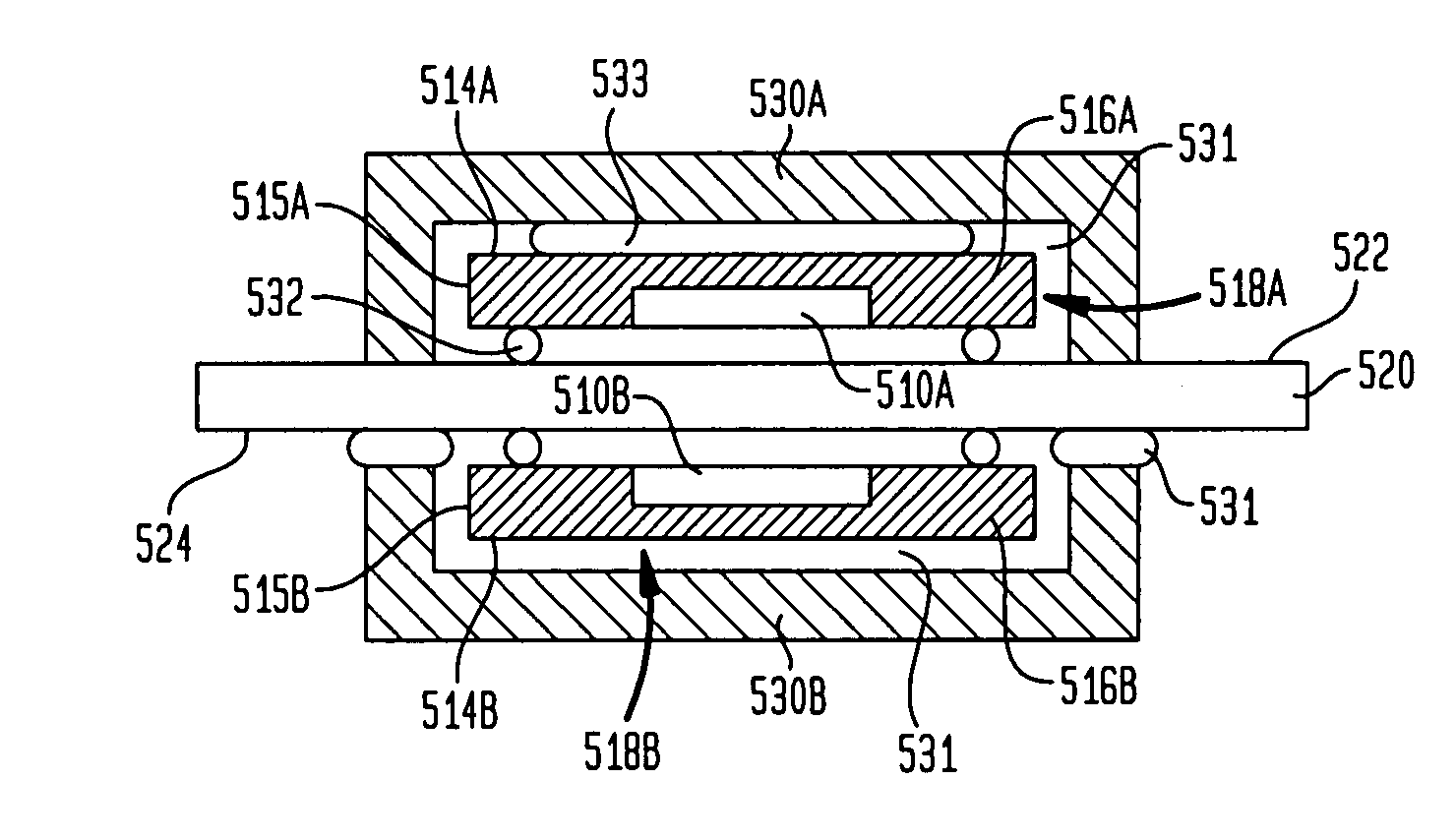
Various structures chip packages are disclosed including a magnetoresistive random access memory (“MRAM”) device and a magnetic shield structure. The magnetic shield structure may be made from material having either ferromagnetic or diamagnetic material and may be shaped and incorporated into the chip package to divert stray magnetic fields away from the MRAM device.

Description

BACKGROUND OF THE INVENTION[0001]This application claims the benefit of the filing date of U.S. Provisional Patent Application No. 60 / 851,646 filed Oct. 13, 2006, the disclosure of which is incorporated herein by reference.[0002]The following application includes the article Gao and Honer, “Magnetic Shielding for Stacked MRAM”, Semiconductor Packaging, Dec. 1, 2006 which is incorporated by reference herein.[0003]Magnetoresistive random access memory (“MRAM”) is a form of computer memory which uses magnetic polarity to store data. The use of magnetic polarity is advantageous because it results in a non-volatile form of memory, which means that it does not necessarily require an electrical current to retain the data stored therein. A typical MRAM structure uses many individual cells, each formed of two layers of ferromagnetic material separated by a thin layer of an insulating material. Each cell is capable of storing one bit of memory, which is carried out by imparting either a posit...

Claims


Application Information

Patent Timeline
Patent Type & Authority Applications(United States)
IPC IPC(8): H01L23/552
CPCH01L23/552H01L2225/107H01L27/222H01L2224/16H01L2224/48091H01L2224/4824H01L2924/01078H01L2924/15311H01L2924/15331H01L2924/3025H01L25/105H01L2225/1058H01L24/48H01L2225/1023H01L2924/00014H01L2924/00011H10B61/00H01L2224/0401H01L2224/45099H01L2224/45015H01L2924/207
Inventor HONER, KENNETH ALLENGAO, GUILIANCARLSON, WILLIAM WALTERWARNER, MICHAEL
Owner TESSERA INC
Learn More