
Partially stacked semiconductor devices

a semiconductor and chip technology, applied in semiconductor devices, semiconductor/solid-state device details, electrical equipment, etc., can solve the problems of long connection path between lsi chips, low footprint efficiency on circuit boards, and inability to select a known good die (kgd) separately, so as to reduce the feature size of wiring connections, increase the number of connections, and shorten the connection path

Inactive Publication Date: 2008-05-29
KK TOSHIBA
View PDF8 Cites 0 Cited by
  • Summary
  • Abstract
  • Description
  • Claims
  • Application Information

AI Technical Summary

Benefits of technology

[0015]One advantage of the invention is that the feature size of the wiring connection can be significantly smaller than those done by wire bonding. Other advantages of the invention include the increased number of connections between LSI chips and the shortened connection path, both of which can facilitate high performance. Moreover, by selectively using the KGD, embodiments of the invention can improve yield and avoid the typical drawbacks of the aforementioned prior techniques.

Problems solved by technology

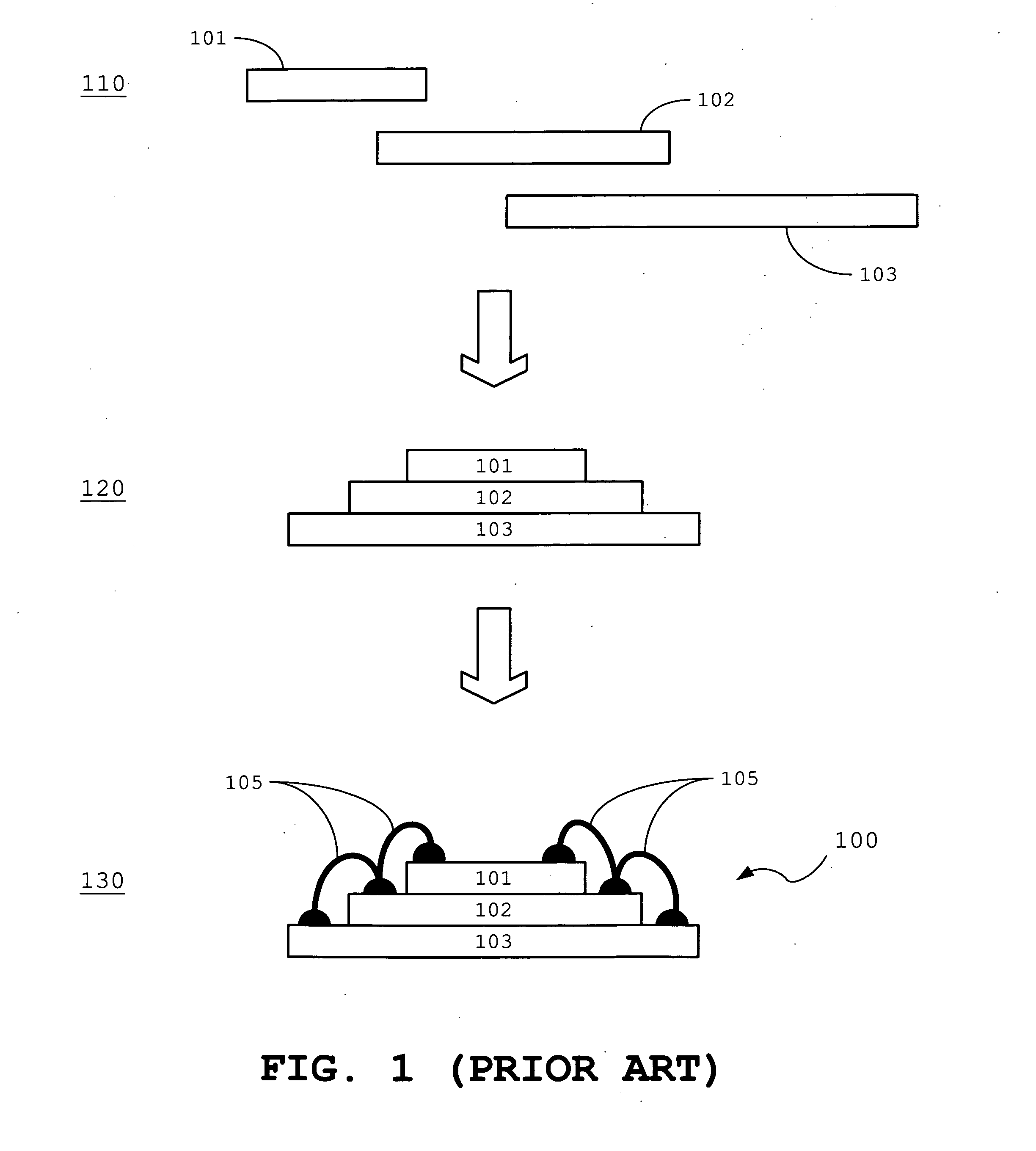
This conventional technique has several drawbacks, including the low footprint efficiency on the circuit board and the long connection path between LSI chips.
Furthermore, the number of connections between LSI chips is limited by the wire bonding pad density.
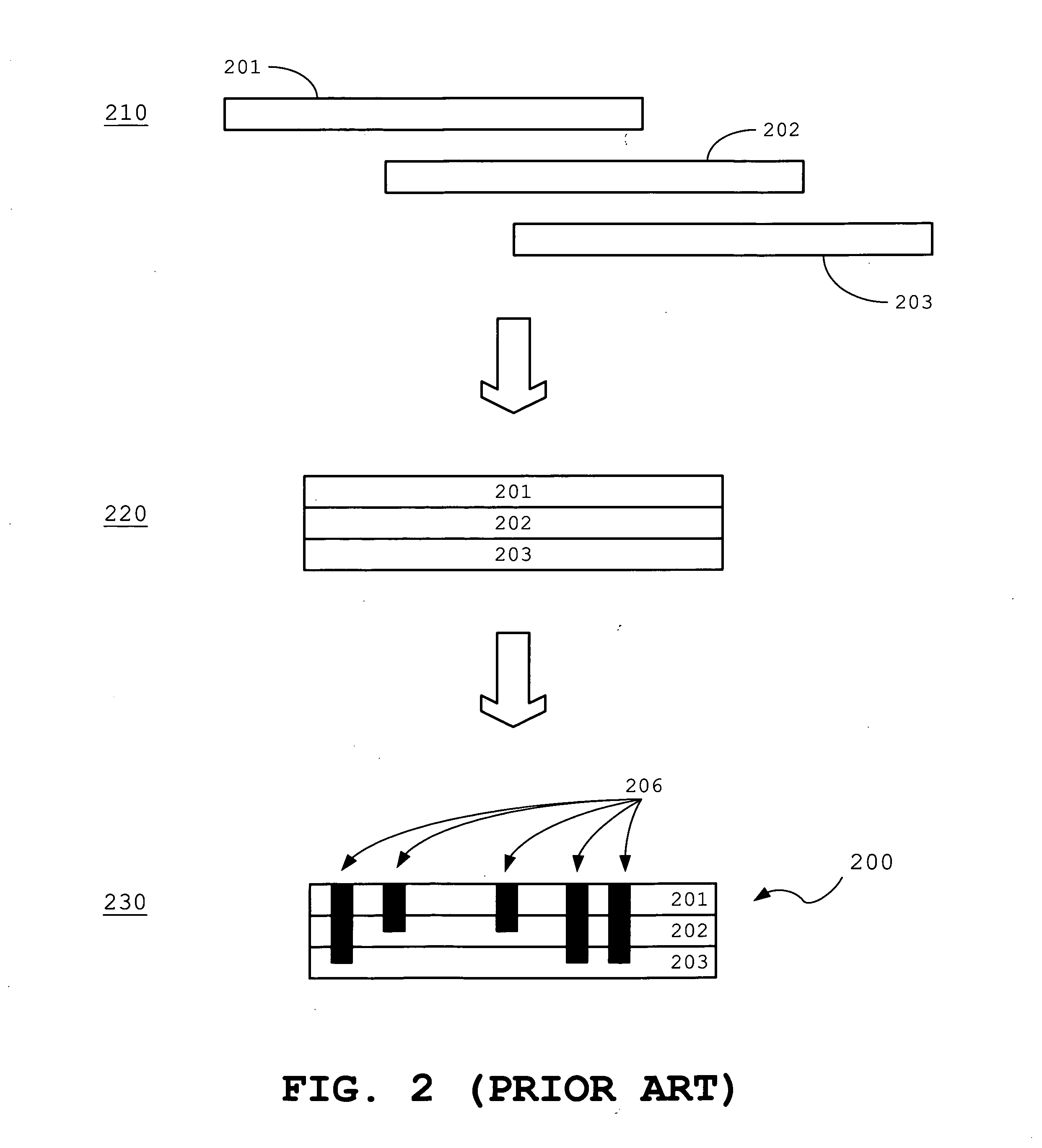
However, due to wafer-wafer bonding, known good die (KGD) cannot be selected separately.

Method used


Image

  • Partially stacked semiconductor devices
  • Partially stacked semiconductor devices
  • Partially stacked semiconductor devices

Examples


Embodiment Construction

[0021]The present invention and various features and advantageous details thereof will now be described with reference to the exemplary, and therefore non-limiting, embodiments that are illustrated in the accompanying drawings. Descriptions of known techniques and technologies may be omitted so as not to unnecessarily obscure the invention in detail. It should be understood, however, that the detailed description and the specific examples, while indicating preferred embodiments of the invention, are given by way of illustration only and not by way of limitation. Figures are not drawn to scale. Various substitutions, modifications, additions and / or rearrangements within the spirit and / or scope of the underlying inventive concept will become apparent to those skilled in the art from this disclosure.

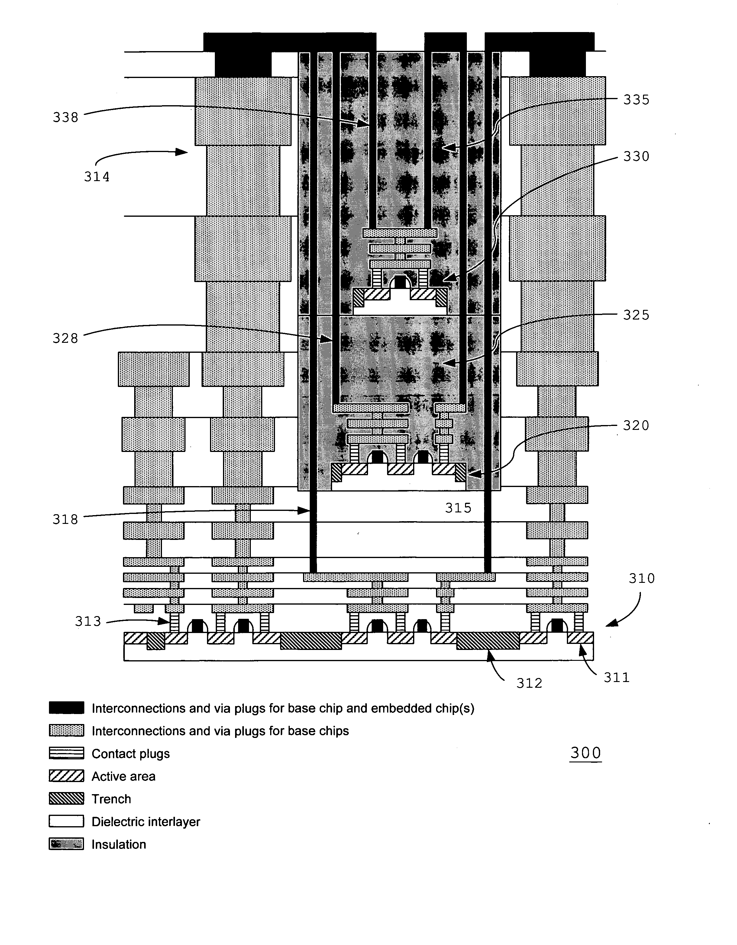
[0022]FIG. 3 is a cross sectional view of a schematic representation of a partially stacked semiconductor device 300 according to one embodiment of the invention. In this example, partially...


PUM


Abstract

Embodiments of the present invention provide partially stacked semiconductor devices and methods of making the same. In one embodiment, a first LSI chip is strategically buried or embedded in a second LSI chip. One embodiment of a method of making a partially stacked semiconductor device may comprise digging a trench on an area of a diced LSI chip where upper metal interconnects do not exist, placing a known good die in the trench, and applying a coating insulator material to fix the position of the embedded chip. The latter two steps may be repeated. The inter-chip connection between the partially stacked LSI chips can be fabricated by forming through holes connecting the chips and filling the through holes with metal.

Description

FIELD OF THE INVENTION[0001]This invention relates generally to semiconductor devices. More particularly, embodiments of the present invention relate to partially stacked semiconductor devices and methods of making the same.BACKGROUND OF THE INVENTION[0002]Semiconductor manufacturing processes generally involve three stages: crystal wafer growth and preparation, wafer fabrication, and final assembly. The last stage has to do with assembling and packaging the fabricated wafer for final product. During this stage, semiconductor chips may undergo several operations or processes. The order and number of processes can vary, depending upon the package type and other known factors. Semiconductor assembly and packing processes may include separating and sorting the fabricated wafers, mounting and bonding the wafers to appropriate support media (e.g., a circuit board), electrically interconnecting the semiconductor in the package, and preparation the final package.[0003]In some cases, partic...

Claims


Application Information

Patent Timeline
Patent Type & Authority Applications(United States)
IPC IPC(8): H01L23/02H01L21/02
CPCH01L25/0657H01L2224/32145H01L2224/48091H01L2225/06527H01L2225/06555H01L2924/00014
Inventor INOHARA, MASAHIRO
Owner KK TOSHIBA
Learn More