
Data Processing System

a data processing system and data processing technology, applied in the field of data processing systems, can solve the problems of inability to carry out real-time processing, inability to simulate a complex circuit, and a large amount of testing time, and achieve the effects of high performance, high functioning, and great freedom of trade-offs

Active Publication Date: 2008-05-29
TOKYO KEIKI
View PDF3 Cites 16 Cited by
  • Summary
  • Abstract
  • Description
  • Claims
  • Application Information

AI Technical Summary

Benefits of technology

[0007]In response to the problem of real-time performance, a method called “hardware acceleration” is known. According to this idea, in an initial stage, a plurality of CPUs or DSPs are aligned and operated in parallel and by assigning small-scale circuits to each, the overall simulation time can be reduced. Since FPGAs and PLDs have become available, methods that directly assign the circuit to be simulated to such devices have become predominant, with it becoming possible to emulate large-scale integrated circuits or hardware with performance that is extremely close to real-time performance.
[0038]That is, in the present invention, a feasible dynamic optimization technology of a hardware space is provided. In the present invention, system called an architecture code is provided in which hardware circuit information that has been conventionally provided by a physical entity and software information such as an instruction program that controls a hardware circuit are integrated and encoded as new information. Using the architecture codes, dynamically optimizing in an execution cycle for hardware becomes possible so as to trade off, at each moment, between hardware resources that become effective and the required processing performance under constraint conditions of the application requirements (architecture), and therefore, a reconfigurable chip can beat a dedicated LSI designed for a specified application in terms of all three of chip cost, required performance, and power consumption.

Problems solved by technology

Since real-time processing is also impossible, a great deal of testing time is required to simulate a complex circuit.
For this reason, not only is it impossible to carry out processing in place of a modem special-purpose or dedicated LSI that has a huge number of gates, it is also becoming increasingly difficult to test the functions of complex dedicated LSIs.
However, the internal cell construction of an FPGA is an architecture where a certain amount of time is required to change the hardware circuit realized by the FPGA, and therefore FPGA are not suited to implementing hardware with data paths, such as a CPU or a DSP.
In fact, when such hardware is implemented on an FPGA, it is not possible to compete with a specially designed LSI in terms of any of processing performance (operation frequency), gate efficiency, and power consumption.
Also, depending on the circuit for executing an application, when an FPGA or PLD is used and the scale of the circuit to be implemented exceeds the degree of integration of the FPGA or PLD, as a rule such implementation will not be possible.
Although it would be conceivable to implement the circuit for executing the application by dividing the circuit, in such case a plurality of chips are used, and due to the limited number of pins, performance, cost and power consumption become even worse.

Method used


Image

  • Data Processing System
  • Data Processing System
  • Data Processing System

Examples


Embodiment Construction

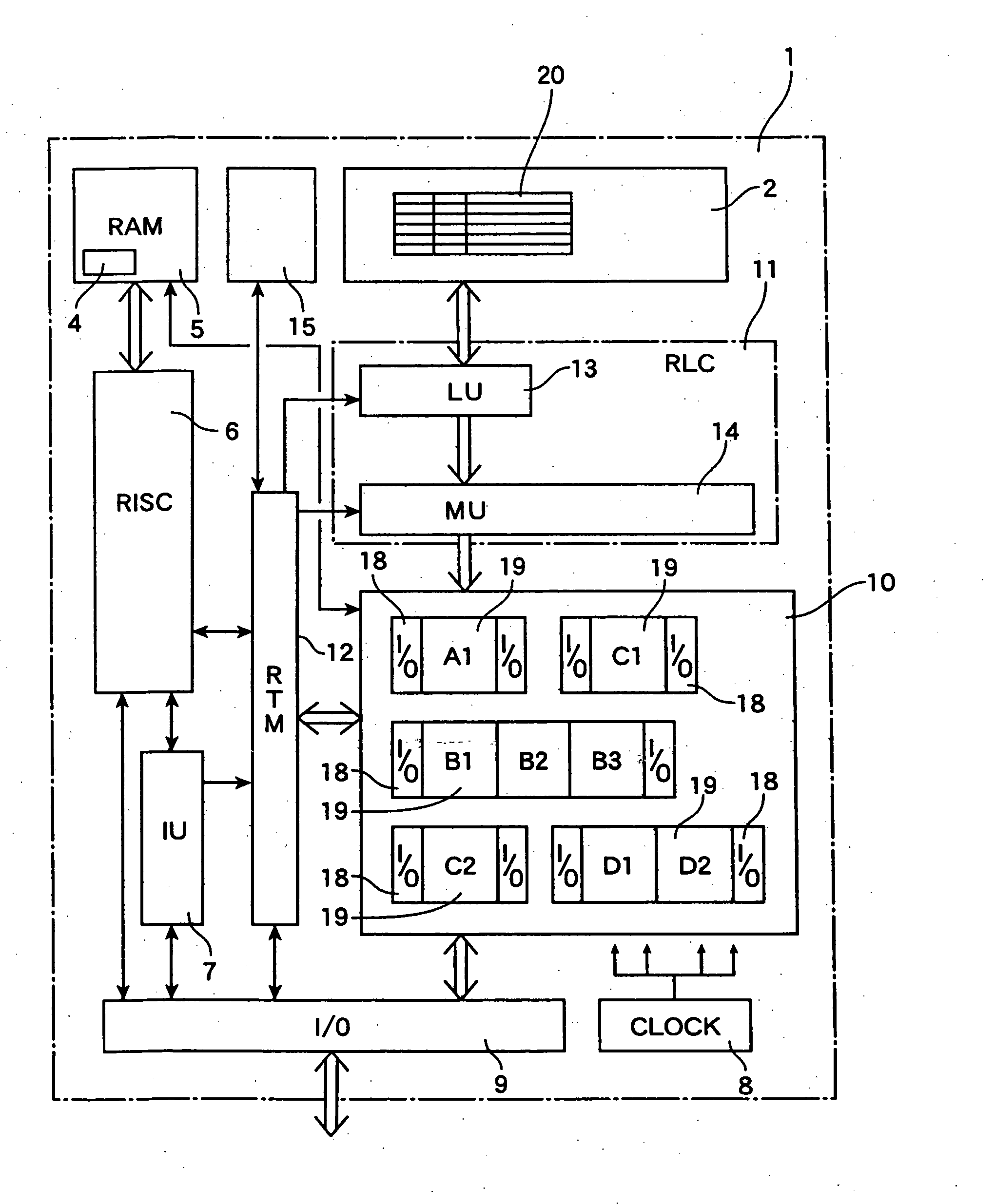
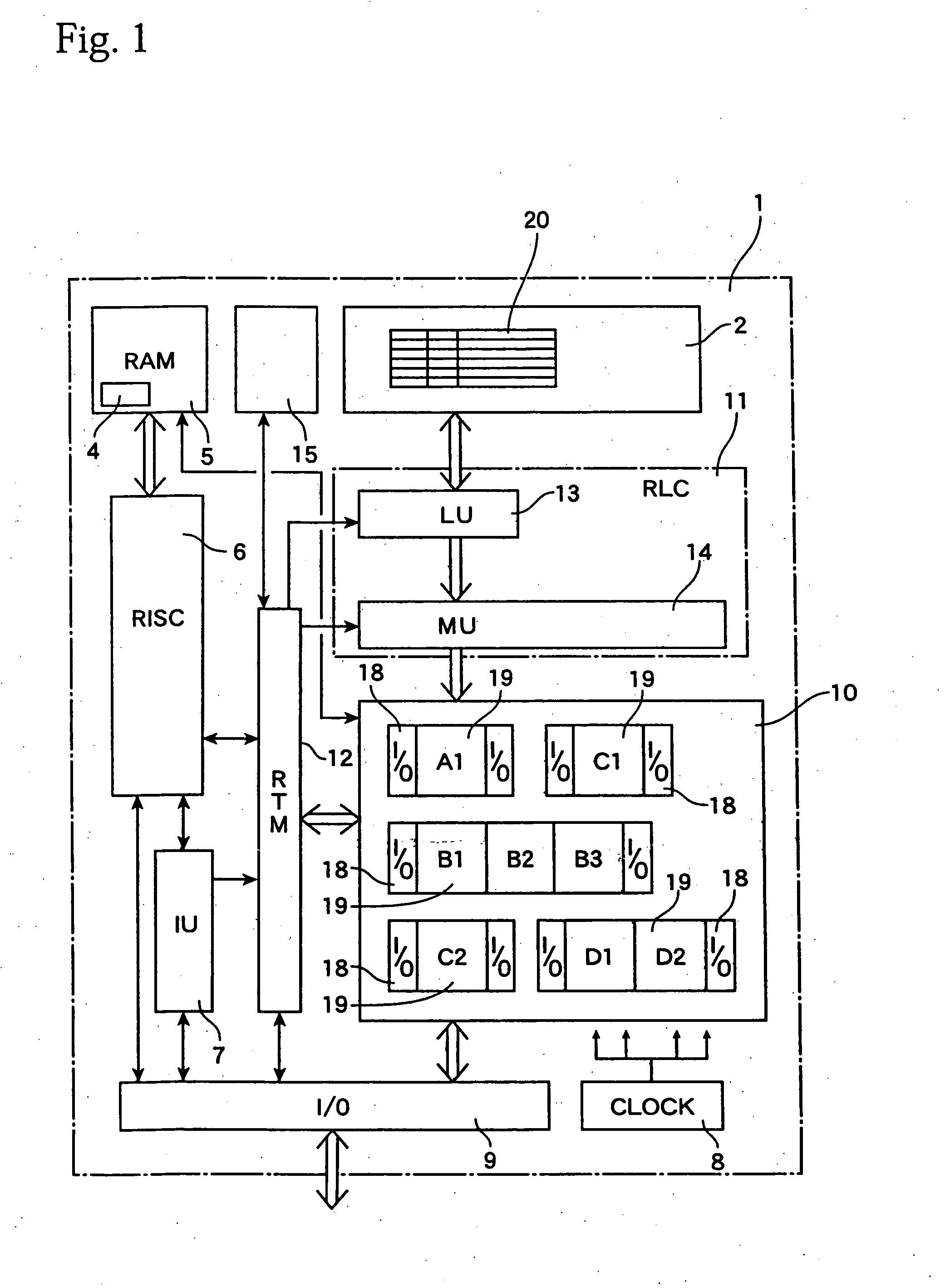
[0059]FIG. 1 shows one of a data processing system included in the present invention. The data processing system (apparatus or device) 1 is an architecture LSI and includes a logic circuit region (“RC region” or “reconfigurable region”) 10 where circuits can be dynamically reconfigured, an architecture library 2 in which a number of architecture codes 20 of hardware modules are stored, a rapid loading control unit (RLC) 11 that can translate the architecture codes 20 on the reconfigurable hardware 10 and initialize and execute the divisional hardware, and a rapid logic communication master (RTM) 12 that can carry out control of a rapid logic circuit exchanging operation and transmission (transfer) of hierarchical information. The RLC 11 includes a function as a load unit (LU) 13 that obtains (i.e., fetches or downloads) the architecture codes 20 from the library 2. In addition, the RLC 11 includes a function as a mapping unit (MU) 14 that carries out mapping of object circuits 19 an...


PUM


Abstract

The present invention provides an architecture code 20 including object circuit information 23 for mapping an object circuit that is at least part of a circuit for executing an application onto part of a logic circuit where circuits can be dynamically reconfigured, interface circuit information 24 for mapping an interface circuit in contact with the object circuit onto the logic circuit, and boundary condition 26 to be realized in the interface circuit. A data processing system in the present invention includes a load unit obtaining an architecture code 20, a mapping unit for mapping the object circuit and the interface circuit in contact with the object circuit onto the logic circuit region according to the object circuit information 23 and the interface circuit information 24 of the architecture code, and a behavior control unit for controlling the interface circuit according to the boundary condition 26 of the architecture code.

Description

TECHNICAL FIELD[0001]The present invention relates to a data processing system with a reconfigurable logic circuit region.BACKGROUND ART[0002]Devices called FPGAs (Field Programmable Gate Arrays), PLDs (Programmable Logic Devices), and PLAs (Programmable Logic Arrays) are known as programmable devices where circuits can be reconfigured. Such programmable devices are fundamentally constructed by disposing units called logic cells or logic units in a lattice and disposing sets of wires so as to surround such units, with it being possible to change the functions of the logic cells or the connections of the wires based on information called context information or configuration information.[0003]As one example of a technique for implementing parts of a logic circuit in FPGAs, Japanese Laid-Open Patent Publication No. 2000-40745 discloses a technique where an initial netlist that characterizes a logic circuit is divided into many pages and circuits for one of such pages are configured in ...

Claims


Application Information

Patent Timeline
IPC IPC(8): H03K19/173G06F9/30
CPCG06F15/7867Y02B60/1225Y02B60/1207G06F17/5054G06F30/34Y02D10/00G06F9/00G06F9/30H03K19/173
Inventor SATO, TOMOYOSHI
Owner TOKYO KEIKI
Learn More