Laminated electronic component and method for manufacturing the same

a technology of laminated electronic components and manufacturing methods, applied in the direction of fixed capacitor details, stacked capacitors, fixed capacitors, etc., can solve the problems of inability to contact the internal electrodes of electrically conductive media during electroplating, disadvantageous decrease in effective volume rate, and complicated steps of applying conductive paste at specific locations, etc., to achieve outstanding humidity resistance and high effective volume rate

Active Publication Date: 2008-05-29
MURATA MFG CO LTD
View PDF25 Cites 135 Cited by
  • Summary
  • Abstract
  • Description
  • Claims
  • Application Information

AI Technical Summary

Benefits of technology

[0013]To overcome the problems described above, a preferred embodiment of the present invention provides a method for manufacturing a laminated electronic component, which has a

Problems solved by technology

A step of applying this conductive paste at specific locations is very complicated.
Furthermore, since the thickness of the conductive paste is relatively large, the effective volume rate is disadvantageously decreased.
In addition, in the method disclosed in Japanese Unexamined Patent Application Publication No. 2004-146401, if the conductive paste is not formed, since the ends of the internal electrodes of the laminate are withdrawn from the exposed surface before the plating is performed, a problem may arise in that electrically conductive media are not likely to be in contact with the internal electrodes during the electroplating.
In this case, not only is the plating efficiency co

Method used


Image

  • Laminated electronic component and method for manufacturing the same
  • Laminated electronic component and method for manufacturing the same
  • Laminated electronic component and method for manufacturing the same

Examples


experimental example 1

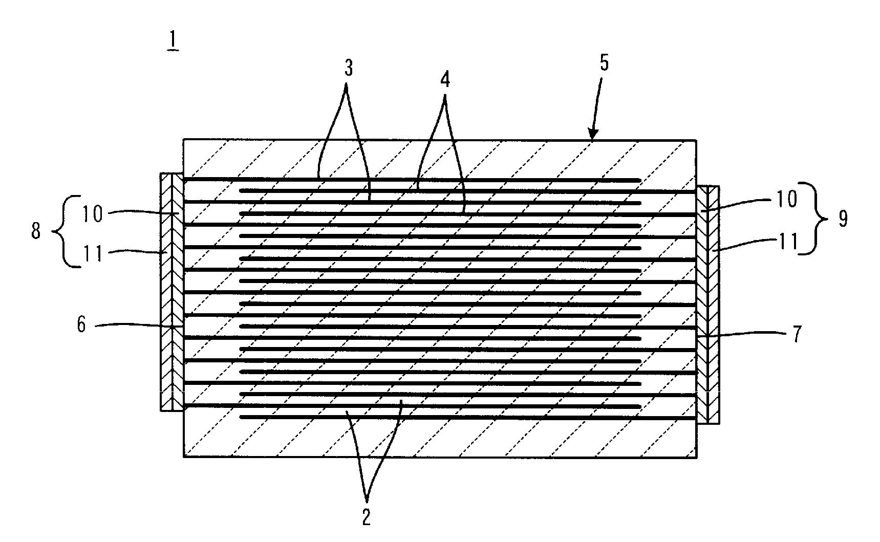
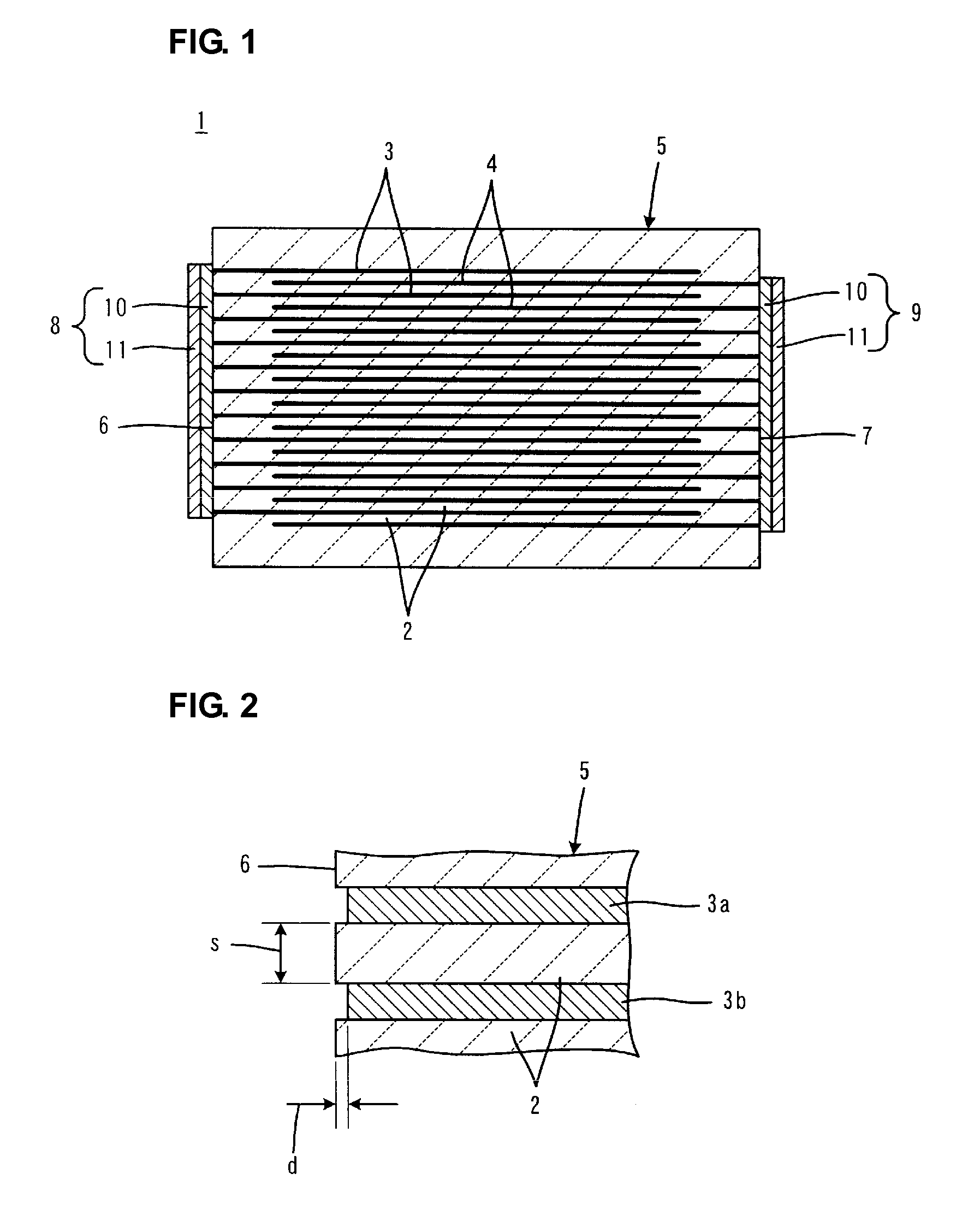
[0098]In Experimental Example 1, after laminates used for a laminated electronic component as shown in FIG. 1 were prepared in which the space “s” between internal electrodes and the withdrawn distance “d” or the protruding length “p”, shown in FIG. 2 or 6, were variously changed, Ni plating layers were directly formed on individual end surfaces, and further Sn plating layers were formed on the Ni plating layers, so that the plating progress was investigated.

[0099]More specifically, as a plating substrate, a laminate for a laminated ceramic capacitor having a length of about 3.2 mm, a width of about 1.6 mm, and a thickness of about 1.6 mm was prepared, in which insulating layers were made of a barium titanate dielectric material, and the internal electrodes were primarily made of Ni. In addition, as for the space “s” of the adjacent internal electrodes, two types were prepared having spaces of about 10 μm and about 13 μm, which were each measured at a location having the largest spa...

experimental example 2

[0109]In Experimental Example 2, when the Ni plating layers were directly formed on the end surfaces of the laminate for the laminated electronic component, various brightening agents were added to the respective Ni plating Watt baths, and the effects thereof were investigated.

[0110]As a plating substrate, the same laminates used for the laminated ceramic capacitor in Experimental Example 1 were prepared. In this laminate, the space “s” between the adjacent internal electrodes was about 10 μm which was measured at a location having a largest space.

[0111]Next, a sandblasting treatment was performed for each laminate, and the withdrawn distance “d” of the internal electrodes with respect to the end surface of the laminate at which the internal electrodes were exposed was set to about 0.1 μm at a location having a largest distance.

[0112]On the other hand, as shown in Table 2, 9 types of Ni plating Watt baths including various brightening agents, which were used for Samples 11 to 19, we...

experimental example 3

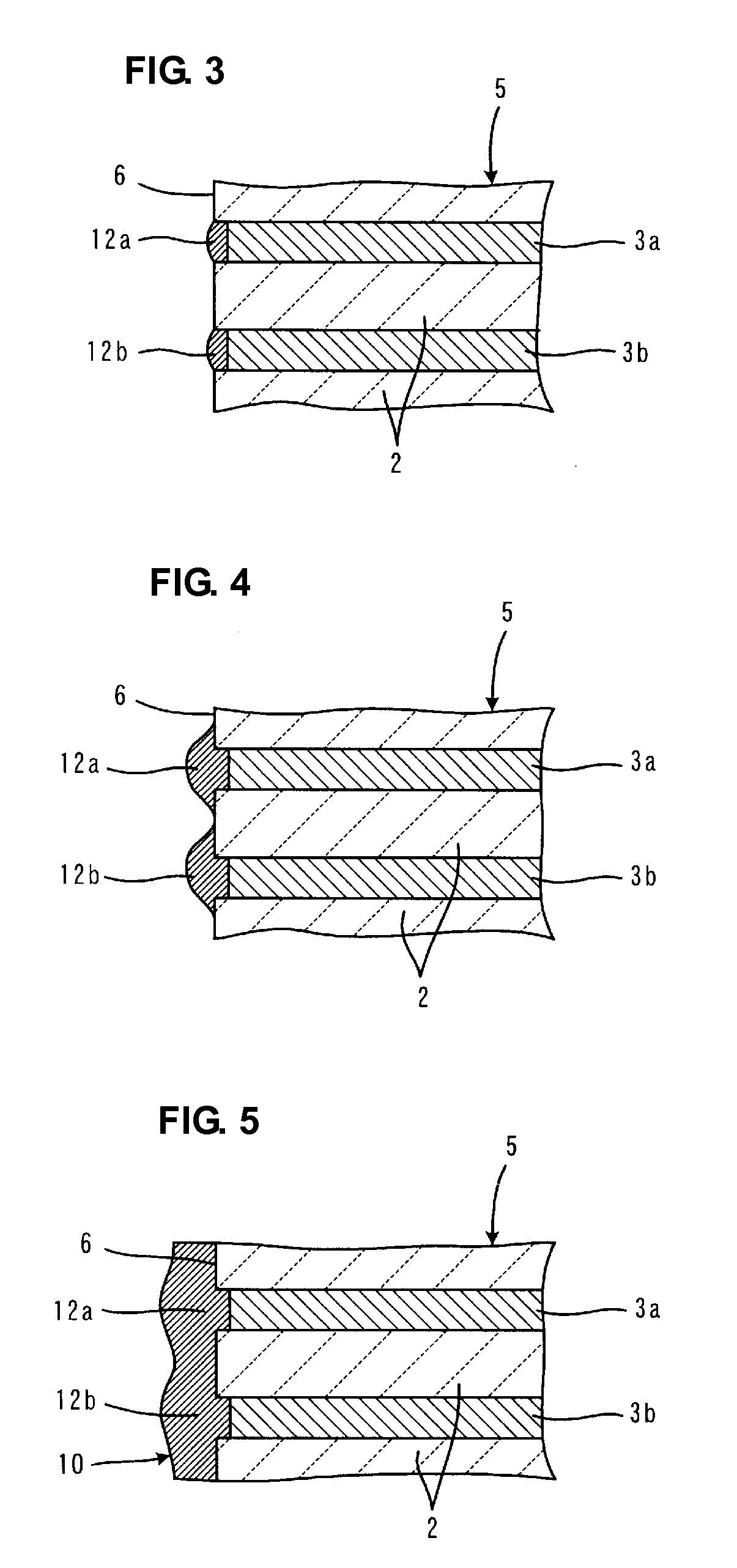
[0118]In Experimental Example 3, after Cu plating layers were directly formed on a surface of a laminate used for a laminated ceramic capacitor having the structure as shown in FIG. 8 at which internal electrodes were exposed, Ni plating layers and Sn plating layers were further formed, so that the completed laminated ceramic capacitor was formed.

[0119]More specifically, as a plating substrate, a laminate for a laminated ceramic capacitor, which included insulating layers made of a barium titanate dielectric material and internal electrodes primarily made of Ni, was prepared. The above laminate had a length of about 3.2 mm, a width of about 1.6 mm, and a thickness of about 1.6 mm; one of two surfaces of the laminate, which were defined as the length direction dimension and the thickness direction dimension, was used as a surface on which external electrodes were to be formed; and the internal electrodes were exposed at two predetermined locations of the above one surface. The space ...


PUM

PropertyMeasurementUnit
Thicknessaaaaaaaaaa
Thicknessaaaaaaaaaa
Lengthaaaaaaaaaa

Abstract

A laminate is prepared in which adjacent internal electrodes are electrically insulated from each other at an end surface at which the internal electrodes are exposed, a space between the adjacent internal electrodes, which is measured in the thickness direction of insulating layers, is about 10 μm or less, and a withdrawn distance of the adjacent internal electrodes from the end surface is about 1 μm or less. In an electroplating step, electroplating deposits deposited on the ends of the adjacent internal electrodes are grown so as to be connected to each other.

Description

BACKGROUND OF THE INVENTION[0001]1. Field of the Invention[0002]The present invention relates to a laminated electronic component and a method for manufacturing the same, and more particularly relates to a laminated electronic component, which includes external electrodes directly provided on external surfaces of a laminate by plating, and to a method for manufacturing the same.[0003]2. Description of the Related Art[0004]As shown in FIG. 11, a laminated electronic component 101, represented by a multilayer ceramic capacitor, includes a laminate 105 including insulating layers 102 laminated to each other and layer-shaped internal electrodes 103 and 104 which are arranged along interfaces between the insulating layers 102. Ends of the internal electrodes 103 and ends of the internal electrodes 104 are exposed at one end surface 106 and the other end surface 107 of the laminate 105, respectively, and external electrodes 108 and 109 are arranged so as to be electrically connected betwe...

Claims


Application Information

Patent Timeline
IPC IPC(8): H01G4/228
CPCC25D3/12C25D5/02C25D7/00C25D21/10H01G4/2325Y10T29/49147Y10T29/435Y10T29/49126Y10T29/49204Y10T29/49163H01G4/30
Inventor KUNISHI, TATSUOTAKANO, YOSHIHIKOKURODA, SHIGEYUKIMOTOKI, AKIHIROKASHIO, HIDEYUKINOJI, TAKASHI
Owner MURATA MFG CO LTD
Why Eureka
Try Eureka