Semiconductor circuit, scanning circuit and display device using these circuits

a scanning circuit and semiconductor technology, applied in the direction of digital storage, instruments, pulse automatic control, etc., can solve the problems of low current driving capability of transistor mb>2/b>, high added value and high cost, and achieve the effect of improving the margin of circuit operation

Active Publication Date: 2008-05-29
BEIHAI HKC OPTOELECTRONICS TECH CO LTD
View PDF19 Cites 34 Cited by
  • Summary
  • Abstract
  • Description
  • Claims
  • Application Information

AI Technical Summary

Benefits of technology

[0053]Accordingly, an object of the present invention is to provide a semiconductor circuit that improves the margin of circuit operation with respect to fluctuations in transistor characteristics without increasing the number of clock signals, a scan circuit having this semiconductor circuit and a display device having the scan circuit.
[0065]In the present invention, refresh is performed using a signal having a period shorter than that of the clock signal. As a result, an abnormal output due to a change in potential at a floating node does not occur. This makes it possible to improve the robustness of a semiconductor device to leakage.

Problems solved by technology

In the past, polysilicon TFTs (thin-film transistors) formed on an insulating substrate required expensive quartz substrates owing to the high-temperature processes involved in manufacture.
Such TFTs have been applied to display panels of small size, and high added value and expensive.
Consequently, the current driving capability of transistor M2 declines, as a result of which it is difficult to hold GOUT[N] in an OFF state.
That is, in Patent Document 2, erroneous operation in which an output is produced at a timing at which output is unnecessary is brought about by leakage current from the transistor.
This leads to fluctuations in transistor characteristics.
When it is attempted to implement the circuit of Patent Document 2 using thin-film transistors, therefore, there are cases where the circuit malfunctions owing to the fluctuation in transistor characteristics.
With the arrangement of Patent Document 3, however, a separate problem arises, namely an increase in the number of clock signals.
Consequently, because the arrangement described in Patent Document 3 is implemented by thin-film transistors, either the problem of circuit malfunction due to fluctuations in transistor characteristics or the problem of an increase in number of clock signals is the result.

Method used


Image

  • Semiconductor circuit, scanning circuit and display device using these circuits
  • Semiconductor circuit, scanning circuit and display device using these circuits
  • Semiconductor circuit, scanning circuit and display device using these circuits

Examples


first example

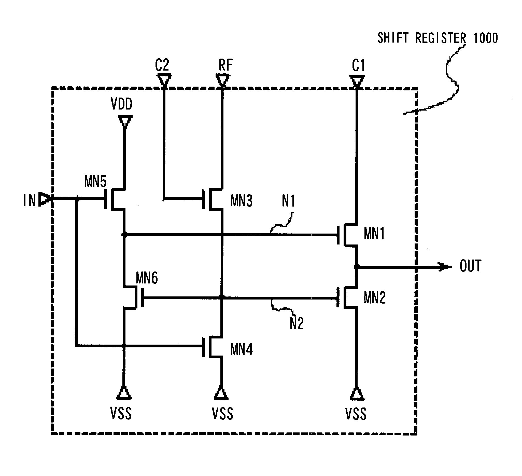
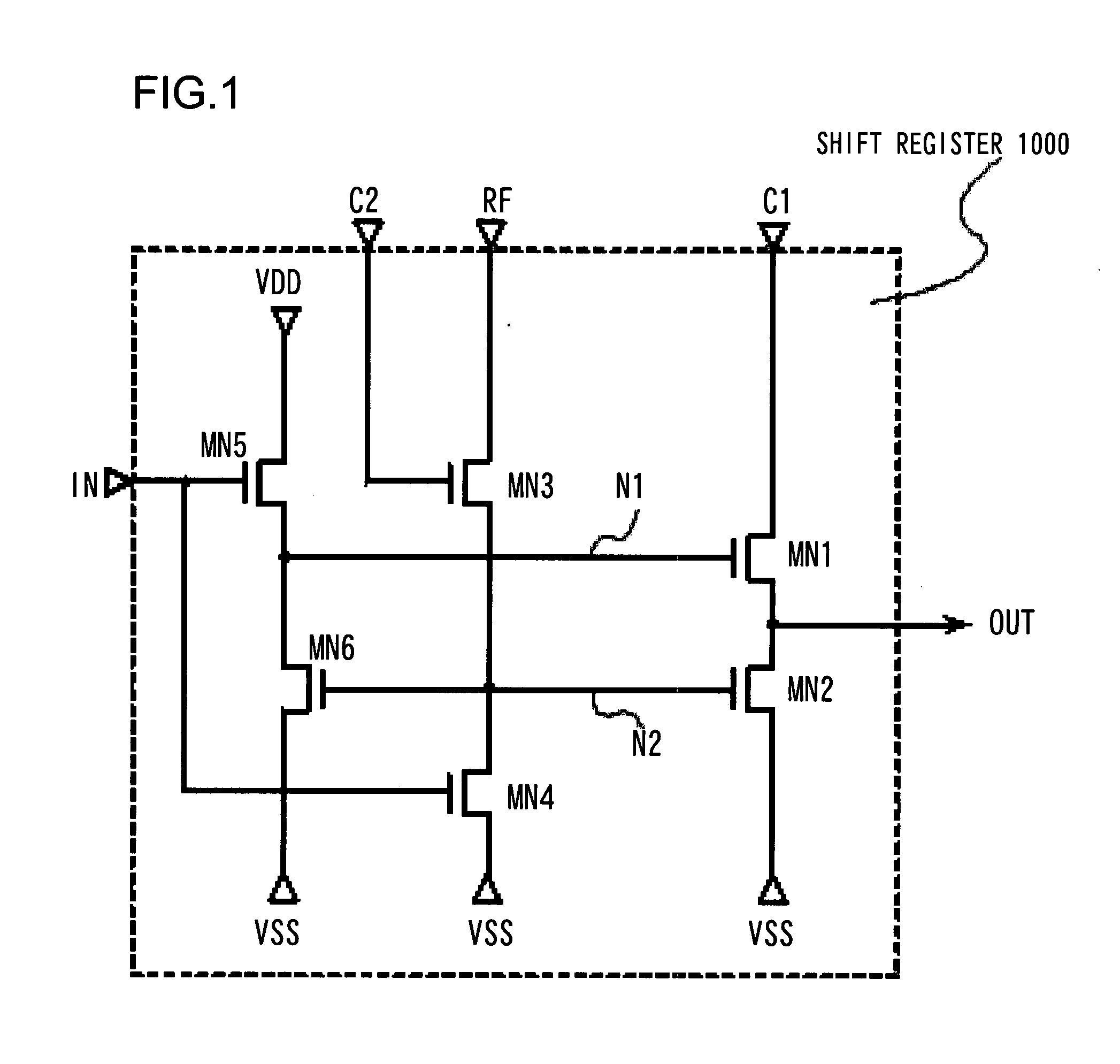
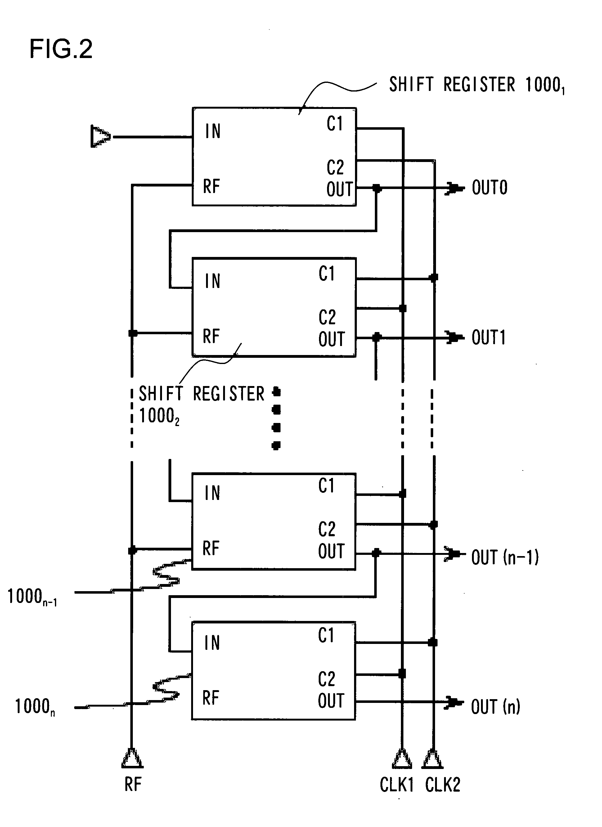
[0091]FIG. 1 is a diagram illustrating the arrangement of a semiconductor circuit according to a first example of the present invention, and FIG. 2 is a diagram illustrating an example of an arrangement in which a shift register (semiconductor circuit) 1000 shown in FIG. 1 is provided as a basic circuit unit. The physical shape and size of each N-channel MOS transistor (referred to as an NMOS transistor) may be designed within limits in which circuit operation is possible with a sufficient operating margin.

[0092]In the example illustrated in FIG. 1, though it does not represent any particular limitation, as control signals, first and second clock signals (CLK1 and CLK2) are input from first and second clock terminals C1, C2, respectively, a start signal (ST) is input from a signal input terminal IN and a refresh signal (RF) is input from a terminal RF, and an output signal (OUT) is output from an output terminal OUT. More specifically, as shown in FIG. 1, the shift register 1000 inc...

second example

[0122]FIG. 5 is a diagram illustrating the arrangement of a second example of the present invention. The structural difference between this example and the first example is the polarity (conductivity type) of the transistors that construct the shift register 1000. Whereas the shift register is composed of NMOS transistors MN1 to MN6 in the first example, it is composed of PMOS transistors MP1 to MP6 in this example.

[0123]The physical shape and size of each P MOS transistor may be designed within limits in which circuit operation is possible with a sufficient operating margin. An OUT signal is output by inputting clock signals CLK1, CLK2, start signal ST and refresh signal RF as control signals.

[0124]As in the first example, the shift register 1000 in this example also has the configuration shown in FIG. 2.

[0125]FIG. 6 is a timing chart for describing the operation of this example. The operation of this example will be described with reference to FIGS. 2, 5 and 6.

[0126]First, when th...

third example

[0145]The structure of a third example of the present invention will be described next. FIG. 8 is a diagram illustrating the arrangement of a third example of the present invention. As illustrated in FIG. 8, this example is such that the shift register 10001, which is the basic structural unit, is composed of NMOS transistors (MN01 to MN07).

[0146]FIG. 8 illustrates an arrangement in which two of the shift registers 1000 are connected together to form two stages. The structure of the shift register 10001 of the first stage comprises the components of FIG. 1 described above as the first example.

[0147]The structural difference between the shift register 10002 of the second stage (and subsequent stages) and the shift register 10001 of the first stage is the portion having cascode-connected NMOS transistors MN13 and MN17.

[0148]In the shift register 10001 of the first stage, a transistor MN03 controlled using the signals RF and CLK2 is connected to the RF terminal and a node N02. From the...


PUM


Abstract

Disclosed is a semiconductor circuit in which a floating node is set to any voltage by utilizing a control signal which is applied to a refresh terminal and has a period shorter than that of a clock signal. The semiconductor circuit includes first and second transistors connected between a first clock terminal and a first power supply terminal, third and fourth transistors connected between the refresh terminal and the first power supply terminal, and fifth and sixth transistors connected between a second power supply terminal and the first power supply. Gates of the fourth and fifth transistors are connected in common to an input terminal, a gate of the third transistor is connected to a second clock terminal, a gate of the first transistor is connected to a connection node between the fifth and sixth transistors, the gate of the second transistor is connected to the gate of the sixth transistor, and a connection node between the first and second transistors is connected to an output terminal.

Description

REFERENCE TO RELATED APPLICATION[0001]This application is based upon and claims the benefit of the priority of Japanese patent application No. 2006-318634, filed on Nov. 27, 2006, the disclosure of which is incorporated herein in its entirety by reference thereto.FIELD OF THE INVENTION[0002]This invention relates to a semiconductor circuit and to a semiconductor device using this circuit. More particularly, the invention relates to a semiconductor circuit constructed using thin-film transistors that are only N-channel transistors or only P-channel transistors.BACKGROUND OF THE INVENTION[0003]An typical active-matrix type liquid crystal display combined with an active-matrix type driver circuits on a same substrate will be described. For forming driver circuits on the same substrate of a display panel, the polysilicon TFTs are applied in manufacture processes. In the past, polysilicon TFTs (thin-film transistors) formed on an insulating substrate required expensive quartz substrates ...

Claims


Application Information

Patent Timeline
Patent Type & Authority Applications(United States)
IPC IPC(8): G11C19/28H03L5/00
CPCG11C19/28
Inventor OTOSE, TOMOHIKO
Owner BEIHAI HKC OPTOELECTRONICS TECH CO LTD
Why Eureka
Try Eureka