Check patentability & draft patents in minutes with Patsnap Eureka AI!

Method for decapsulating package

a technology of decapsulation and packaging, applied in the field of semiconductor process, can solve the problems of difficult to remove the underfill, easy damage to the chip surface, and serious damage to the electrical probing during failure inspection

Active Publication Date: 2008-05-29
UNITED MICROELECTRONICS CORP
View PDF13 Cites 6 Cited by
  • Summary
  • Abstract
  • Description
  • Claims
  • Application Information

AI Technical Summary

Benefits of technology

[0007]Accordingly, at least one objective of the present invention is to provide a method for removing an underfill from a chip. By applying the method according to the present invention, the underfill is completely removed without damaging the solder bumps.
[0008]At least another objective of the present invention is to provide a method for removing solder bumps from a chip. By applying the method according to the present invention, the solder bumps are removed without damaging the metal pads on the chip.
[0009]The other objective of the present invention is to provide a method for decapsulating a package without damaging a chip packed therein.
[0033]In the present invention, by applying the method for removing the underfill and the method for removing the solder bumps according to the present invention in the method for decapsulating the package, the underfill can be completely removed without damaging the solder bumps or leaving the underfill residual on the chip and the solder bumps can be removed without damaging the metal pads on the chips. Hence, the performance of the reverse engineering, the rework process or the failure inspection process is not affected by the processes for removing the underfill and the solder bumps. Furthermore, since the solder bumps are removed by utilizing the physical property of the material of the solder bumps, the cost for removing the solder bumps is low.

Problems solved by technology

However, the surface of the chip is easily damaged during the grinding or polishing process.
Therefore, the electrical probing during the failure inspection is seriously affected by the grinding or polishing result.
Therefore, when the underfill is the only part needed to be rework, it is hard to remove the underfill but leave the solder bumps on the chip by using the grinding or polishing process.
However, none of the methods can remove the underfill completely without leaving the underfill residual on the chip or can remove the underfill completely without damaging the solder bumps.
Furthermore, none of the methods can remove the solder bumps without damaging the metal pads on the chip or can remove the solder bumps without spending a lot of money.

Method used


Image

  • Method for decapsulating package
  • Method for decapsulating package
  • Method for decapsulating package

Examples


Embodiment Construction

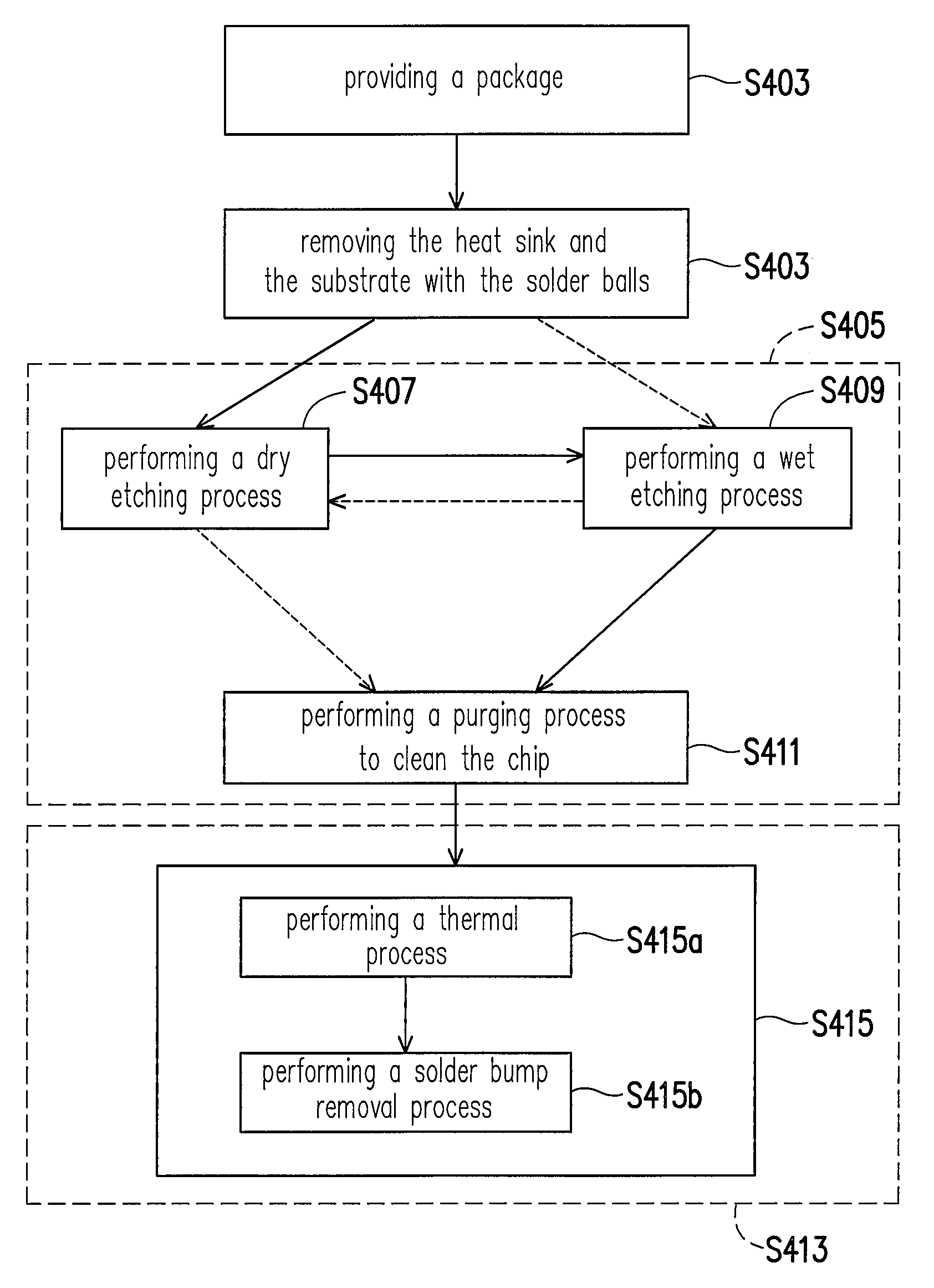
[0040]FIG. 1 is a cross-sectional view schematically illustrating a package. FIG. 2 is a process flow showing a method for removing an underfill from a chip according to one embodiment of the present invention. As shown in FIG. 1, a package 1 is provided. The package 1 can be, for example, a flip-chip package. Furthermore, the package 1 comprises a chip 100 and a substrate 106. The chip 100 further comprises an active surface 100a and a rear surface 100b. The chip 100 is disposed over the substrate 106 in a way that the active surface 100a is opposite to the substrate 106. There are several solder bumps 102 are disposed on the active surface of the chip 100 and between the chip 100 and the substrate 106. That is, the substrate 106 is connected to the chip 100 through the solder bumps 102. Also, an underfill 104 is further disposed between the substrate 106 and the chip 100 and filling between the solder bumps 102. Moreover, on the rear surface 100b of the chip 100, there is a heat s...


PUM

PropertyMeasurementUnit
temperatureaaaaaaaaaa
pressureaaaaaaaaaa

Abstract

A method for decapsulating a package is provided. The method comprises steps of providing a package having a chip therein, wherein the chip has an active surface and a rear surface. Further, the package further comprises a heat sink, a plurality of solder bumps, a substrate, an underfill and a plurality of solder balls. The method further comprises removing the heat sink and removing the substrate together with the solder balls. A dry etching process is performed to remove a portion of the underfill. A wet etching process is performed to remove the rest portion of the underfill. A thermal process solder bump removal process is performed to melt the solder bumps and then a solder bump removal process is performed to remove the melted solder bumps from the active surface of the chip.

Description

BACKGROUND OF THE INVENTION[0001]1. Field of Invention[0002]The present invention relates to a semiconductor process. More particularly, the present invention relates to a technology to detection of a method for decapsulating a package.[0003]2. Description of Related Art[0004]Integrated circuit (IC) packaging is a way of separating the IC chips on a wafer after the front-end semiconductor fabrication process, connecting the chips to individual lead frames and encapsulating the chips for a better protection. At present, the most common chip packaging technique includes the flip chip interconnect technology. The method includes providing conductive bumps on the input / output (I / O) contacts of a chip and then flipping over the chip so that the bumps can directly contact a substrate. The major advantages of the flip chip bonding technique are small area occupation, high lead count, short interconnect, low inductance and easy-to-control noise level. As a result, the flip chip package is p...

Claims


Application Information

Patent Timeline
Patent Type & Authority Applications(United States)
IPC IPC(8): H01L21/463
CPCH01L21/56H01L21/563H01L24/98H01L2224/16225H01L2224/32225H01L2224/73204H01L2924/15311H01L2924/00H01L2924/00011H01L2924/00014H01L2924/01322H01L2924/14H01L2924/00012H01L2224/0401
Inventor SHIH, TUNG-YI
Owner UNITED MICROELECTRONICS CORP
Features
  • R&D
  • Intellectual Property
  • Life Sciences
  • Materials
  • Tech Scout
  • Unparalleled Data Quality
  • Higher Quality Content
  • 60% Fewer Hallucinations
Learn More