Closed-loop design for manufacturability process

a closed-loop design and manufacturability technology, applied in the field of design and manufacture of lithographic masks, can solve the problems of greater fidelity in printing, reduced lithographic accuracy, and inability to reproduce the circuit image precisely on the substrate, etc., and achieves the effect of reducing the computational resource requirements of mbopc and reducing the computational resource requirements

Inactive Publication Date: 2008-05-29
IBM CORP
View PDF6 Cites 221 Cited by
  • Summary
  • Abstract
  • Description
  • Claims
  • Application Information

AI Technical Summary

Benefits of technology

[0032]It is another object of the present invention to provide a method of ensuring that the designer's constraints are satisfied during the mask optimization phase.
[0033]A further object of the invention is to provide a data preparation methodology that will meet the design

Problems solved by technology

However, the polygons of the mask transferred to or imaged on the wafer will be smoothed and distorted during the lithographic process of transferring the mask patterns to the wafer, due to a variety of optical effects, as is well-known in the art.
The circuit image on the photomask may not be reproduced precisely on the substrate, in part because of optical effects among transmitted and blocked energy passing through the photomask.
While MBOPC results in greater fidelity in the printed image, the use of MBOPC requires significantly more computational resource than rules-based OPC.
However, there are several drawbacks to this approach.
This development time frame makes it practically impossible to give designers accurate descriptions of the RET and OPC solutions as well as accurate process window models during the design of the chip.
Having designers optimize layouts to inaccurate models and RET/OPC solutions while they are operating under the assumption that they have accurate insight into the patterning process can lead to catastrophic failures and would make manufacturability worst, not better.
Thus, performing a model-based l

Method used


Image

  • Closed-loop design for manufacturability process
  • Closed-loop design for manufacturability process
  • Closed-loop design for manufacturability process

Examples


Embodiment Construction

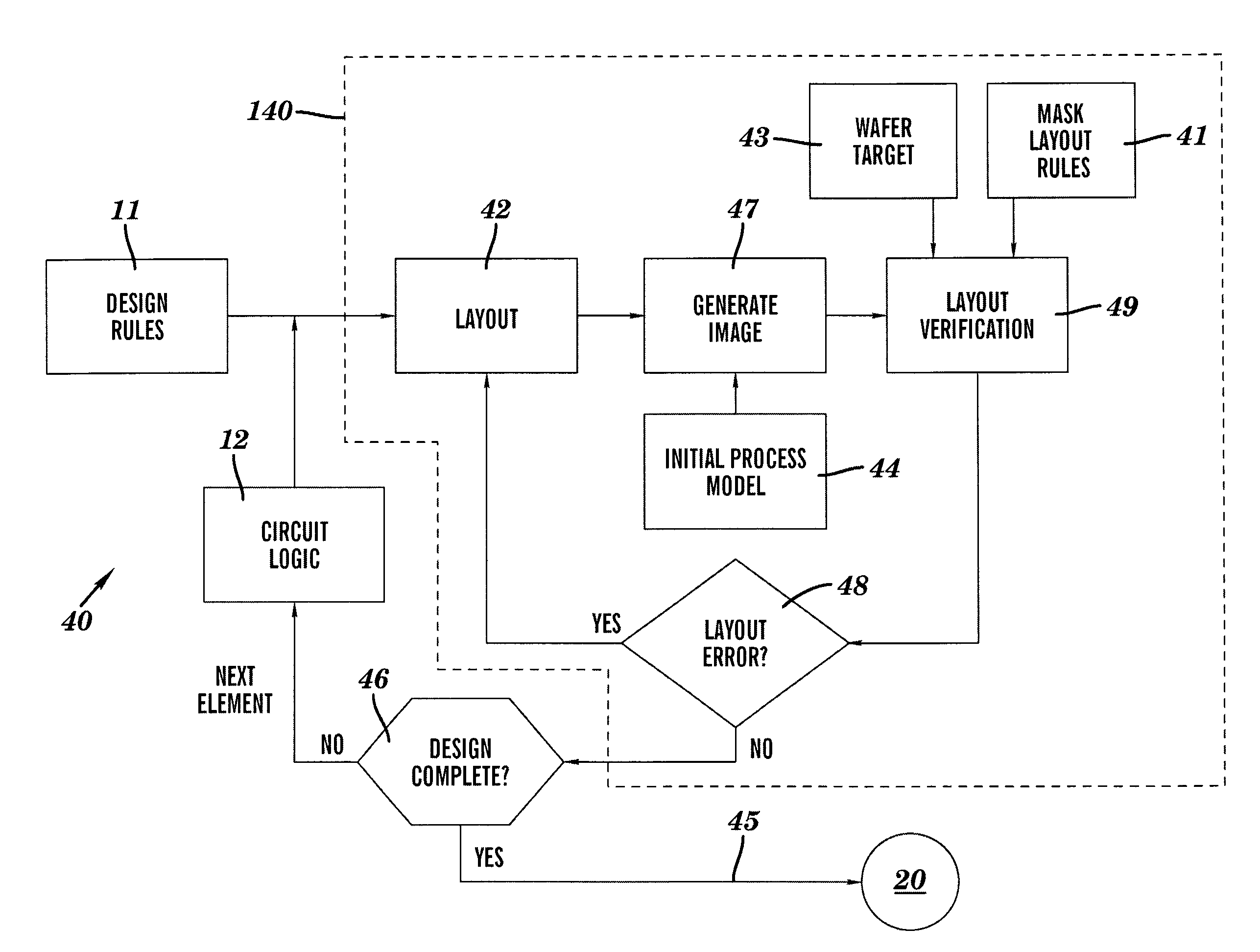
[0058]The present invention will now be described in greater detail by referring to the following discussion with reference to the drawings that accompany the present application. It is observed that the drawings of the present application are provided for illustrative purposes and thus they are not drawn to scale.

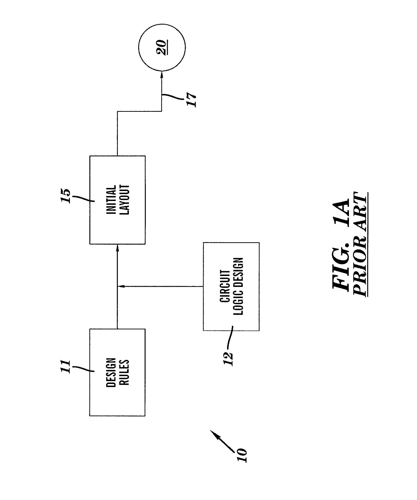
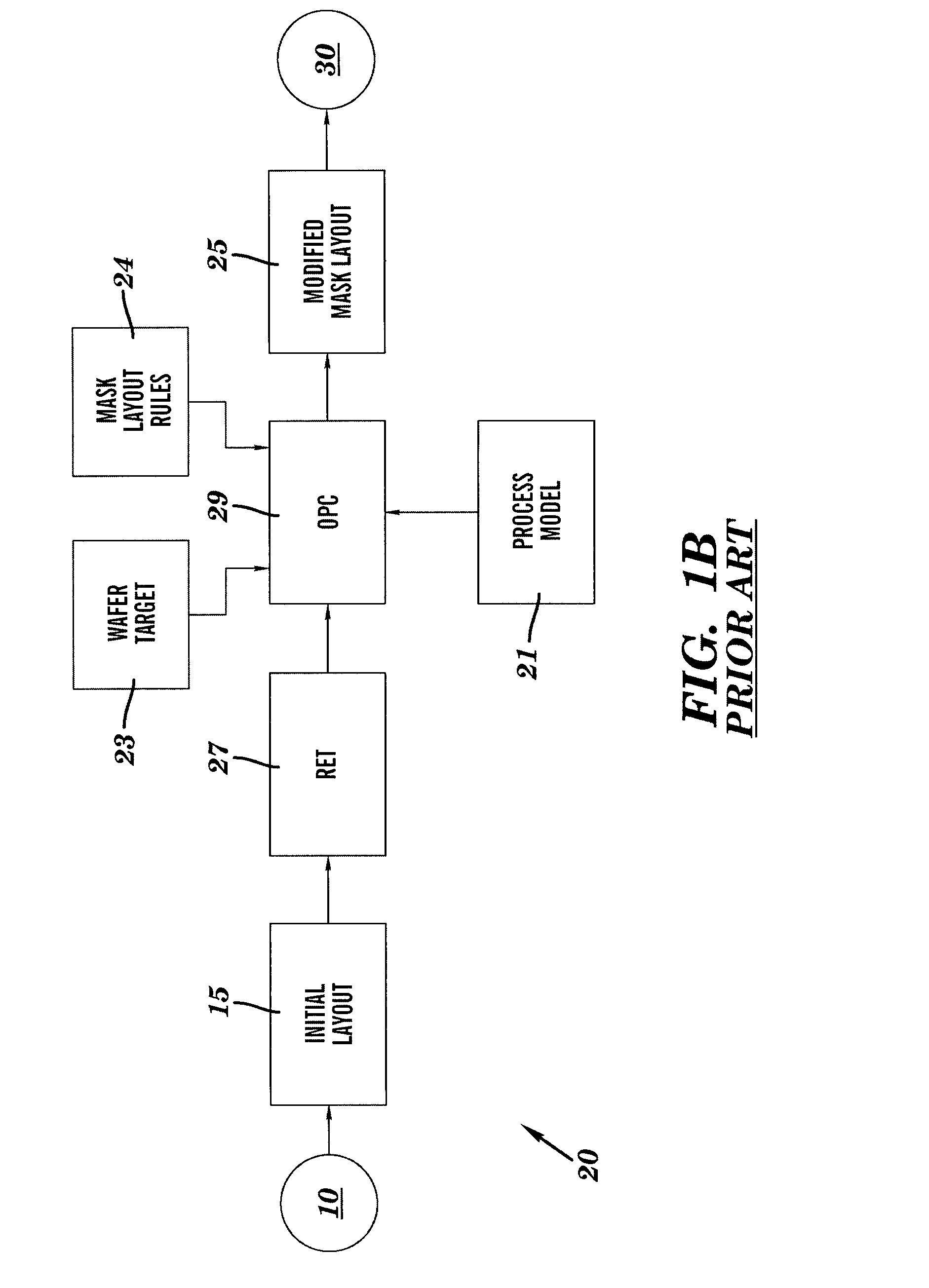
[0059]Referring to FIG. 3, one embodiment of the present invention includes, during a design phase 50 of a circuit layout, circuit logic 12 and design rules 11 are provided and used by a designer, typically with the aid of a variety of software tools (not shown for clarity), to arrive at an initial circuit layout 52. In accordance with the present invention, a layout optimization 350 is performed on the layout 52, or a portion or element of the layout 52, during the design phase which uses a lithographic process model / tool 54, preferably a process window model / tool. The process window model / tool 54 may be similar to a model used by a foundry or fab for OPC. The process win...


PUM


Abstract

A method of designing an integrated circuit is provided in which the design layout is optimized using a process model until the design constraints are satisfied by the image contours simulated by the process model. The process model used in the design phase need not be as accurate as the lithographic model used in preparing the lithographic mask layout during data prep. The resulting image contours are then included with the modified, optimized design layout to the data prep process, in which the mask layout is optimized using the lithographic process model, for example, including RET and OPC. The mask layout optimization matches the images simulated by the lithographic process model with the image contours generated during the design phase, which ensures that the design and manufacturability constraints specified by the designer are satisfied by the optimized mask layout.

Description

FIELD OF THE INVENTION[0001]The present invention relates to the manufacture of integrated circuits and to lithographic methods for manufacturing integrated circuit on a wafer. More particularly, the present invention relates to the design and manufacture of lithographic masks for the manufacture of integrated circuits and a method for optimizing the mask design for manufacturability.BACKGROUND OF THE INVENTION[0002]Integrated circuits are typically fabricated by optical lithographic techniques, where energy beams transmit integrated circuit images or patterns on photomasks (equivalently, masks or reticles) to photosensitive resists on semiconductor wafer substrates, formed (equivalently, printed or transferred) as multiple layers of patterned materials overlain on the substrate. For each patterned layer formed on the substrate, there may be one or more masks used to form the printed patterns on the wafer. The patterns are typically expressed as polygons on the masks. However, the p...

Claims


Application Information

Patent Timeline
IPC IPC(8): G06F17/50
CPCG03F1/36G03F1/144G06F17/00
Inventor GRAUR, IOANAHAN, GENGMANSFIELD, SCOTT M.LIEBMANN, LARS W.
Owner IBM CORP
Why Eureka
Try Eureka