P-type mos transistor, method of forming the same and method of optimizing threshold voltage thereof

a mos transistor and threshold voltage technology, applied in the field of mos transistors, can solve the problems of direct current (dc) failure, non-uniform gate lengths of mos transistors in different directions, and large threat to the yield of products, so as to prevent the non-uniform threshold voltage

Inactive Publication Date: 2008-06-05
SEMICON MFG INT (SHANGHAI) CORP
View PDF4 Cites 1 Cited by
  • Summary
  • Abstract
  • Description
  • Claims
  • Application Information

AI Technical Summary

Benefits of technology

[0006]The embodiments of the present invention provide a P-type MOS transistor and a method for forming the same, and a method of optimizing threshold voltage of a P-type MOS transistor, so as to prevent the non-uniformity in threshold voltages of P-type MOS transistors in a central region (i.e. the region I) and an edge region (i.e. the region II) of a semiconductor substrate.

Problems solved by technology

However, the non-uniformity of the etching may result in non-uniform gate lengths of the MOS transistors in different regions on the semiconductor substrate.
Such a reduction in threshold voltage causes a direct current (DC) failure of the MOS transistors on the edge region, and is a great threat to the yield of the products.
However, the processes are more complicated since the steps of growing polysilicon and photolithography and etching and ion implantation are added.
Further, an additional mask is needed, which increases the processing cycle time and the cost.

Method used


Image

  • P-type mos transistor, method of forming the same and method of optimizing threshold voltage thereof
  • P-type mos transistor, method of forming the same and method of optimizing threshold voltage thereof
  • P-type mos transistor, method of forming the same and method of optimizing threshold voltage thereof

Examples


Embodiment Construction

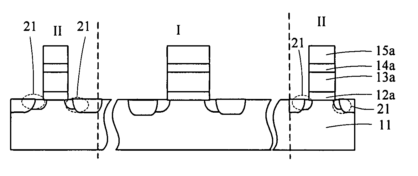
[0030]In the present invention, the doping concentration of source and drain extension regions of a semiconductor substrate is changed by means of a second N-type ion implantation, so as to optimize the threshold voltage of a P-type MOS transistor. The second N-type ion implantation may be performed before forming the P-type MOS transistor, or after forming the P-type MOS transistor, or after source, drain implantation during the process of forming the P-type MOS transistor. In the embodiments of the present invention, the second N-type ion implantation is performed after forming the source and drain of the P-type MOS transistor, which should not unduly limit the scope of the present invention. The location of the second N-type ion implantation is at the source and drain extension regions of the P-type MOS transistor. The dosage of the second N-type ion implantation is determined according to the desired threshold voltage and ranges from 0.7E12 to 1.3E12 cm−2 in the embodiments of t...


PUM


Abstract

The present invention discloses a method of optimizing threshold voltage of P-type MOS transistor, including: providing a semiconductor substrate; forming a P-type MOS transistor on the semiconductor substrate; and performing a second N-type ion implantation in the source and drain extension regions. A P-type MOS transistor and a method for forming the same are also provided, the method includes: providing a semiconductor substrate including a region I and a region II being concentric with the region I and occupying 15% to 25% of the area of the whole semiconductor substrate; forming a P-type MOS transistor on the semiconductor substrate; and performing a second N-type ion implantation in the source and drain extension regions of the region II. Therefore, the reduction in threshold voltage of the P-type MOS transistors in region II of the semiconductor substrate is suppressed.

Description

FIELD OF THE INVENTION[0001]The present invention relates to the field of semiconductor device, particularly to a P-type MOS transistor, a method of forming the P-type MOS transistor and a method of optimizing the threshold voltage thereof.DESCRIPTION OF RELATED ARTS[0002]At present, with the increasing integration of the integrated circuit, the size of device is getting smaller. The feature size of device, which is referred to as the gate length of a MOS transistor, is being scaled down, for example, from 0.13 μm to 0.10 μm. Thus, the gate length of an MOS transistor has a critical impact on the performance of the device. In the prior art, the gate of an MOS transistor is formed by etching the oxide layer, the polysilicon layer, the silicide layer and silicon nitride layer on a semiconductor substrate using plasma. However, the non-uniformity of the etching may result in non-uniform gate lengths of the MOS transistors in different regions on the semiconductor substrate. Particularl...

Claims


Application Information

Patent Timeline
Patent Type & Authority Applications(United States)
IPC IPC(8): H01L29/94H01L21/336
CPCH01L21/26513H01L29/6659H01L21/823456H01L21/823418
Inventor ZHUANG, XIAOHUICHIU, SHENGFENSUN, PENG
Owner SEMICON MFG INT (SHANGHAI) CORP
Why Eureka
Try Eureka