Output Slew Rate Control In Low Voltage Differential Signal (LVDS) Driver
- Summary
- Abstract
- Description
- Claims
- Application Information
AI Technical Summary
Benefits of technology
Problems solved by technology
Method used
Image
Examples
Embodiment Construction
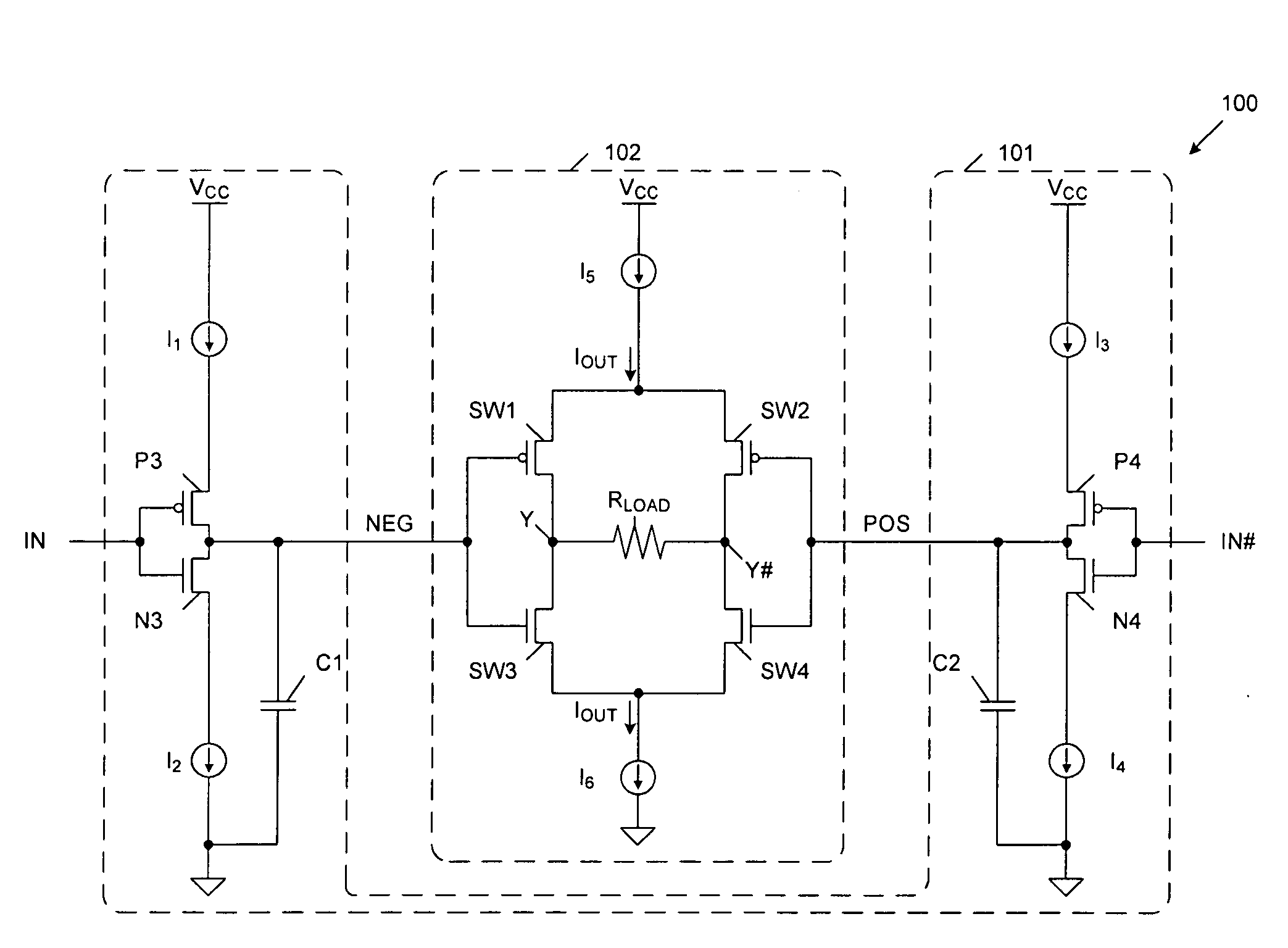
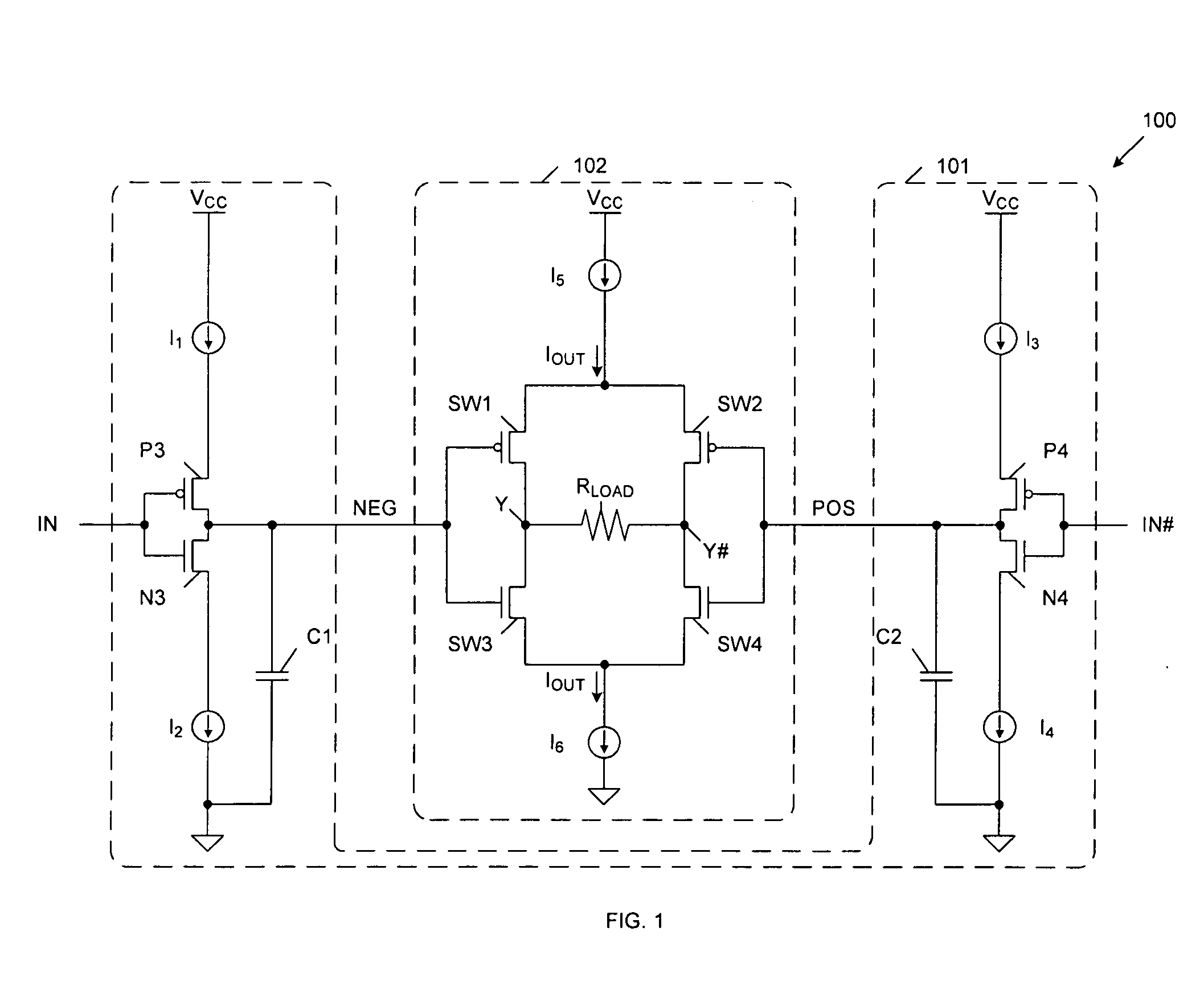
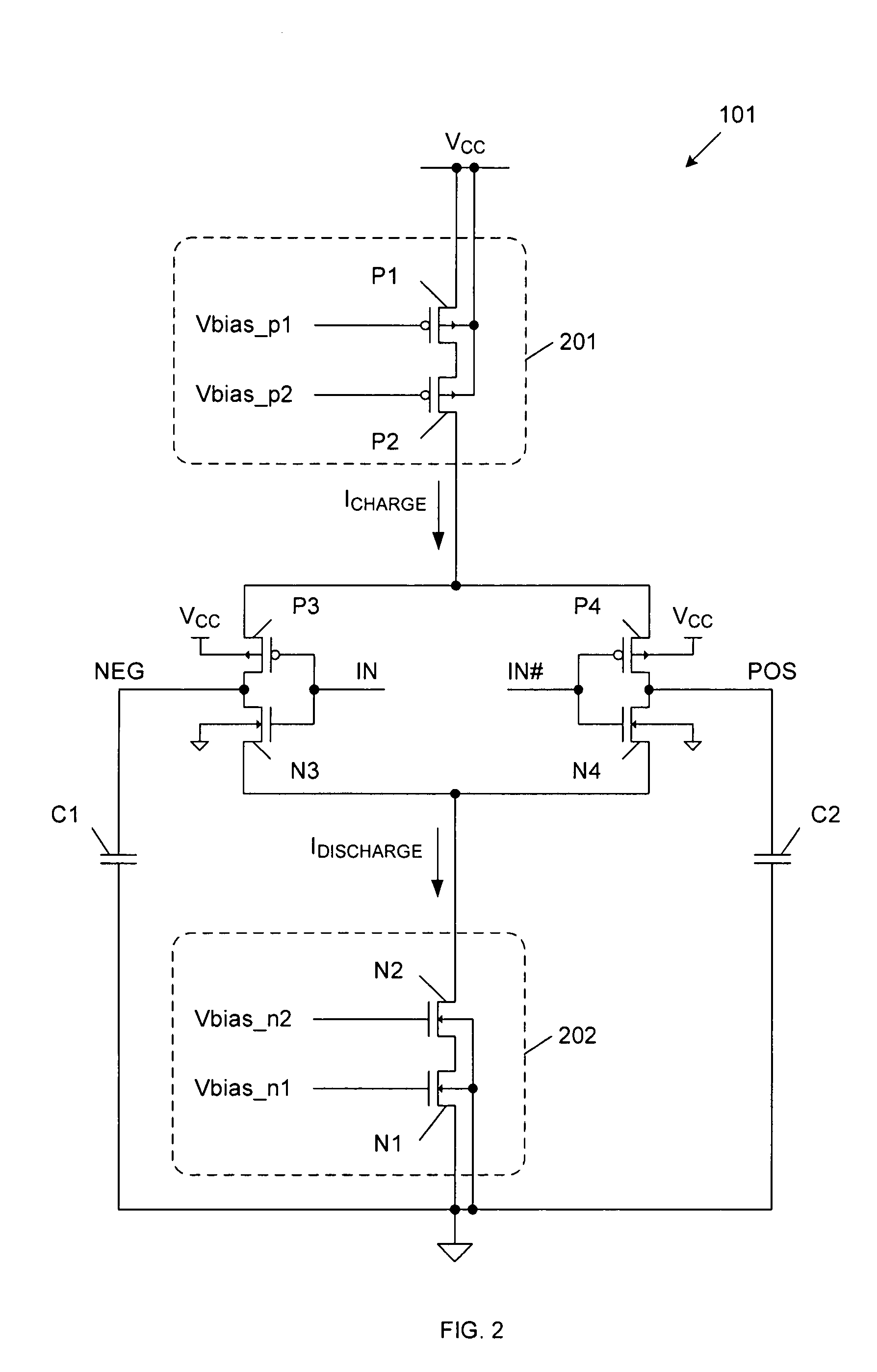
[0017]FIG. 1 is a circuit diagram of a low voltage differential signal (LVDS) driver 100 in accordance with one embodiment of the present invention. LVDS driver 100 includes pre-driver circuit 101 and output driver circuit 102. Pre-driver circuit 101 includes charging current sources I1 and I3, discharging current sources I2 and I4, p-channel transistors P3-P4, n-channel transistors N3-N4, and capacitors C1-C2. Output driver circuit 102 includes output current sources I5-I6, p-channel output switching transistors SW1-SW2, n-channel output switching transistors SW3-SW4 and load resistor RLOAD.
[0018]In general, pre-driver circuit 101 receives a differential input signal, which includes the complementary differential input signals IN and IN#, and in response, generates output control voltages NEG and POS. Driver circuit 102 receives the output control voltages NEG and POS, and in response, drives the differential output voltages on nodes Y and Y#.
[0019]The voltage transitions of the ou...
PUM
 Abstract
Description
Claims
Application Information


