Display apparatus

a technology of display apparatus and display screen, which is applied in the field of display screen, can solve the problems of complex structure of pixel circuits of related art with characteristic fluctuation correction functions, threshold voltage and mobility variations of the transistors driving the light-emitting elements, and adversely affect the light emission luminance, etc., and achieves reduced large layout area of pixels, and high quality

Active Publication Date: 2008-06-05
JOLED INC
View PDF4 Cites 9 Cited by
  • Summary
  • Abstract
  • Description
  • Claims
  • Application Information

AI Technical Summary

Benefits of technology

[0012]According to an embodiment of the present invention, in an active matrix display apparatus wherein light-emitting elements such as organic EL devices are used as pixels, each of the pixels has a function to correct the mobility of the driving transistor, and preferably also has a function to correct the threshold voltage of the driving transistor and a function to correct aging-based variations of the organic EL device (bootstrapping operation) for displaying images of high quality. Heretofore, the pixels with those correcting functions are not suitable for realizing a high-definition display capability due to a large layout area of pixels because the number of components making up the pixels is large. According to the embodiment of the present invention, since the power supply voltage is supplied as switching pulses, the number of components making up the pixels and the number of interconnects used are reduced to reduce the layout area of pixels. The display apparatus can thus be provided as a high-quality, high-definition flat display.
[0013]According to an embodiment of the present invention, in order to render the sampling transistor conductive in a time interval during which the signal line is under the signal potential, the main scanner outputs a control signal having a predetermined pulse duration to the scanning line, thereby holding the signal potential in the retentive capacitor, and simultaneously applies a correction for the mobility of the driving transistor to the signal potential. At this time, the main scanner outputs a power supply pulse having a predetermined pulse duration which is supplied from the pulse power supply as a control signal to the scanning line. Stated otherwise, the main scanner extracts power supply pulses for the respective scanning lines from the train of pulses supplied from the pulse power supply and outputs the extracted power supply pulses as control signals to the corresponding scanning lines. The control signals applied to the gates of the sampling transistors are the power supply pulses, and have accurate pulse waveforms. Since the power supply pulses supplied from the pulse power supply are extracted and supplied to the respective scanning lines, any variations of the control signals between the scanning lines are small for performing a stable sampling process and a stable mobility correcting process. The sampled signal potentials do not suffer variations and there is no danger of luminance irregularities. As a consequence, the display apparatus is capable of displaying images having a good image equality.

Problems solved by technology

However, the active matrix planar self-emission display apparatus of the related art are disadvantageous in that transistors for driving the light-emitting elements suffer from threshold voltage and mobility variations due to fabrication process fluctuations.
Such characteristic variations of the driving transistors and characteristic fluctuations of the organic EL devices adversely affect the light emission luminance.
However, pixel circuits of the related art which have the characteristic fluctuation correcting function are complex in structure as they need interconnects for supplying a correcting potential, switching transistors, and switching pulses.
Since the pixel circuits are made up of many components, they have presented an obstacle to a high-definition display capability.

Method used


Image

  • Display apparatus
  • Display apparatus
  • Display apparatus

Examples


Embodiment Construction

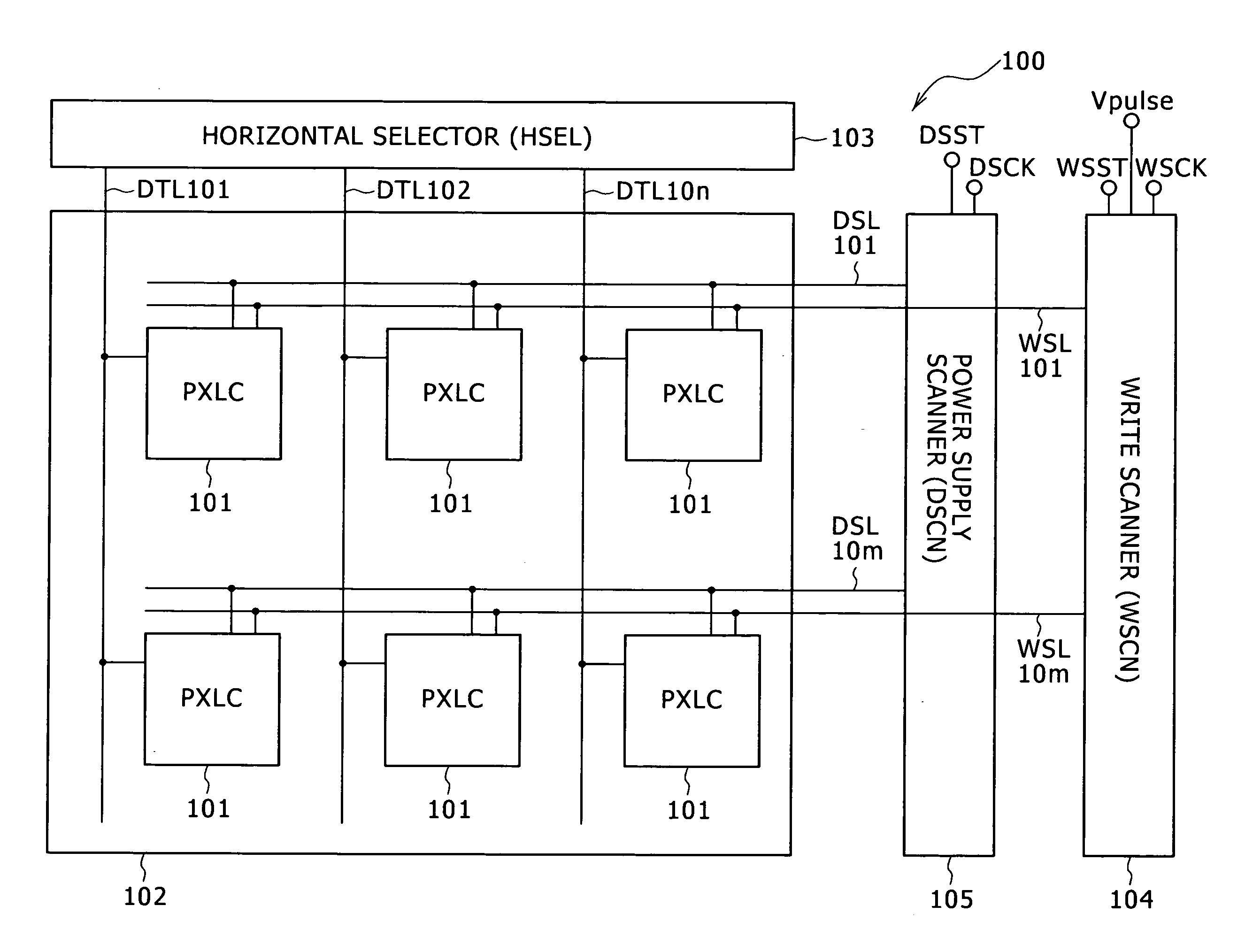
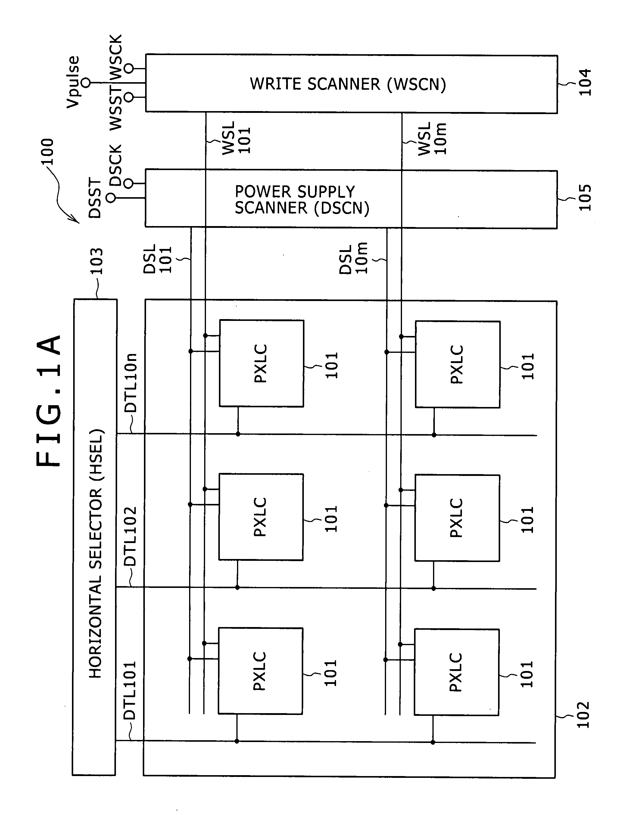
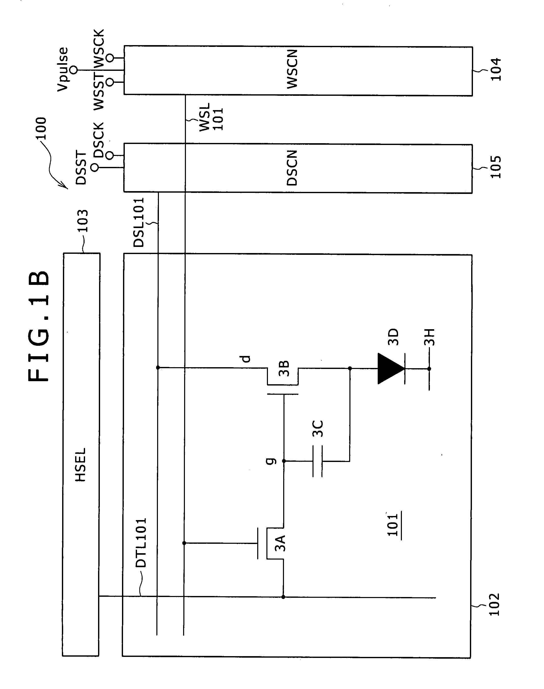
[0024]A display apparatus according to embodiments of the present invention will be described in detail below with reference to the drawings. FIG. 1A shows in block form the display apparatus according to the embodiment of the present invention. As shown in FIG. 1A, the display apparatus, generally designated by 100, includes a pixel array 102 and a driver (103, 104, 105) for driving the pixel array 102. The pixel array 102 includes rows of scanning lines WSL101 through WSL10m, columns of signal lines DTL101 through DTL10n, a matrix of pixels (PXLC) 101 disposed at crossings of the scanning lines WSL101 through WSL10m and the signal lines DTL101 through DTL10n, and feeding lines DSL101 through DSL10m associated with respective rows of the pixels 101. The driver includes a main scanner (write scanner WSCN) 104 for scanning the rows of the pixels 101 in a line sequential mode by supplying a control signal successively to the scanning lines WSL101 through WSL10m, a power supply scanner...


PUM


Abstract

Disclosed herein is a display apparatus including: a pixel array; and a driver configured to drive the pixel array. The pixel array including rows of scanning lines, columns of signal lines, a matrix of pixels disposed at crossings of the scanning lines and the signal lines, and feeding lines associated with respective rows of the pixels, the pixels including respective sampling transistors having respective gates connected to the scanning lines, the driver including a main scanner configured to supply control signals to the scanning lines, the main scanner including a shift register, output buffers connected respectively between the shift register and the scanning lines, and a pulse power supply configured to supply power supply pulses, each having a predetermined pulse duration, to the output buffers, wherein the main scanner outputs power supply pulses supplied from the pulse power supply as the control signals to the respective scanning lines in response to a shift pulse output from the shift register.

Description

CROSS REFERENCES TO RELATED APPLICATIONS[0001]The present invention contains subject matter related to Japanese Patent Application JP 2006-325089 filed in the Japan Patent Office on Dec. 1, 2006, the entire contents of which being incorporated herein by reference.BACKGROUND OF THE INVENTION[0002]1. Field of the Invention[0003]The present invention relates to a display apparatus of the active matrix type including light-emitting elements as pixels.[0004]2. Description of the Related Art[0005]In recent years, growing efforts have been made to develop planar self-emission display apparatus including organic EL devices as light-emitting elements. The organic EL device is a device which utilizes the phenomenon of light emission from an organic thin film that is placed under an electric field. The organic EL device is of a low power requirement as it can be energized under an applied voltage of 10 V or lower. Furthermore, the organic EL device is a self-emission device capable of emitting...

Claims


Application Information

Patent Timeline
Patent Type & Authority Applications(United States)
IPC IPC(8): G09G3/30
CPCG09G3/3233G09G3/3266G09G2320/043G09G2300/0842G09G2300/0866G09G2300/0819G09G3/20G09G3/30G09G3/32G11C19/00
Inventor IIDA, YUKIHITOTOMIDA, MASATSUGUTANIKAME, TAKAOUCHINO, KATSUHIDE
Owner JOLED INC
Why Eureka
Try Eureka