Semiconductor memory device

a memory device and semiconductor technology, applied in the field of semiconductor memory devices, can solve the problems of easy change of power source voltage, large number of refresh defective cells contained in one chip, and easy increase of capacity, so as to reduce power consumption during self-refresh time, effectively relieving refresh defective cells

Active Publication Date: 2008-06-05
LONGITUDE LICENSING LTD
View PDF8 Cites 76 Cited by
  • Summary
  • Abstract
  • Description
  • Claims
  • Application Information

AI Technical Summary

Benefits of technology

[0022]As explained above, according to the present invention, the refresh cycle according to the first refresh mode and the refresh cycle according to the second refresh mode can be independently controlled. Therefore, the refresh operation considering the characteristic in each mode can be executed. For example, when the first refresh mode is the auto-refresh mode and also when the second refresh mode is the self-refresh mode, power consumption during the self-refresh time can be decreased while effectively relieving the refresh defective cells, by narrowing the application range of the multiple refresh during the self-refresh time than the application range of the multiple refresh during the auto-refresh time.

Problems solved by technology

However, along with the progress of miniaturization and a capacity increase, the number of refresh defective cells contained in one chip becomes very large.
Therefore, in recent years, the number of redundant memory cells to be prepared for one chip and the number of fuse elements (ROM) to store defective addresses have become very large, and this interrupts the capacity increase.
However, a power source voltage easily changes by the execution of the read operation or the write operation.
Further, a chip temperature rises due to heat generation by the read operation or the write operation, and there is a possibility that an information holding characteristic of memory cells decreases during the auto-refresh time.
However, because the power consumption permitted in the power down state is very small in the specification, executing a multiple refresh over a wide range has a risk of not satisfying the current standard.
However when the multiple refresh is performed, power consumption during the self-refresh time becomes the problem.
However, the methods described in Japanese Patent Application Laid-open Nos. 2002-157880, 2000-298982, and 2003-68075 are based on the assumption that a part of data is destroyed.
Therefore, it is considered that these methods cannot be applied in substantially all cases.
However, the increase in the power consumption due to the multiple refresh cannot be suppressed.

Method used


Image

  • Semiconductor memory device
  • Semiconductor memory device
  • Semiconductor memory device

Examples


first embodiment

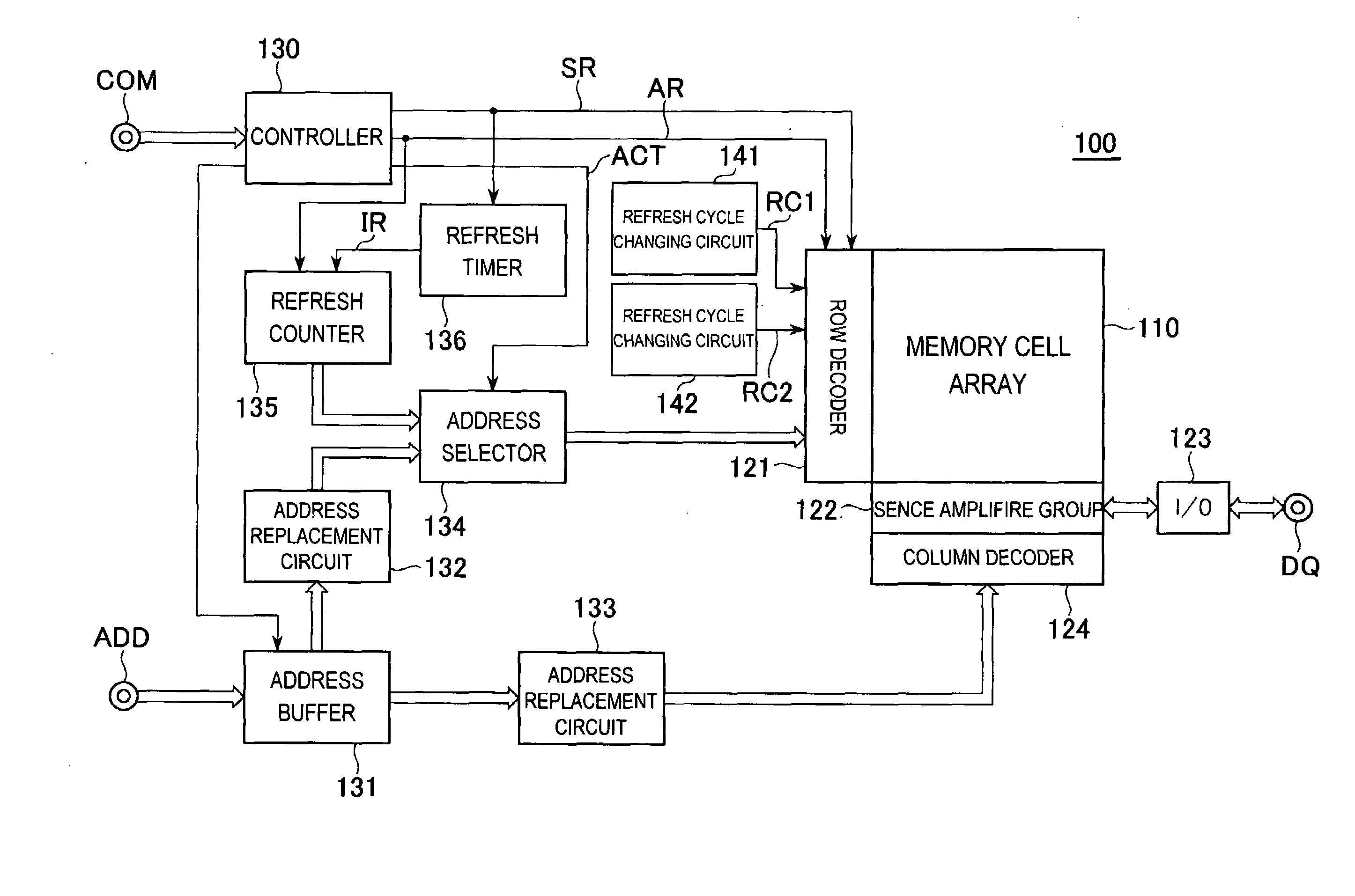
[0038]As shown in FIG. 1, the semiconductor memory device 100 includes a memory cell array 110 having plural memory cells that need to hold information by the refresh operation. The semiconductor memory device 100 has a function (read function) of reading data stored in the address supplied via an address pin ADD, and outputting the read data via a data pin DQ, and a function (write function) of writing data supplied via the data pin DQ to the address supplied via the address pint ADD.

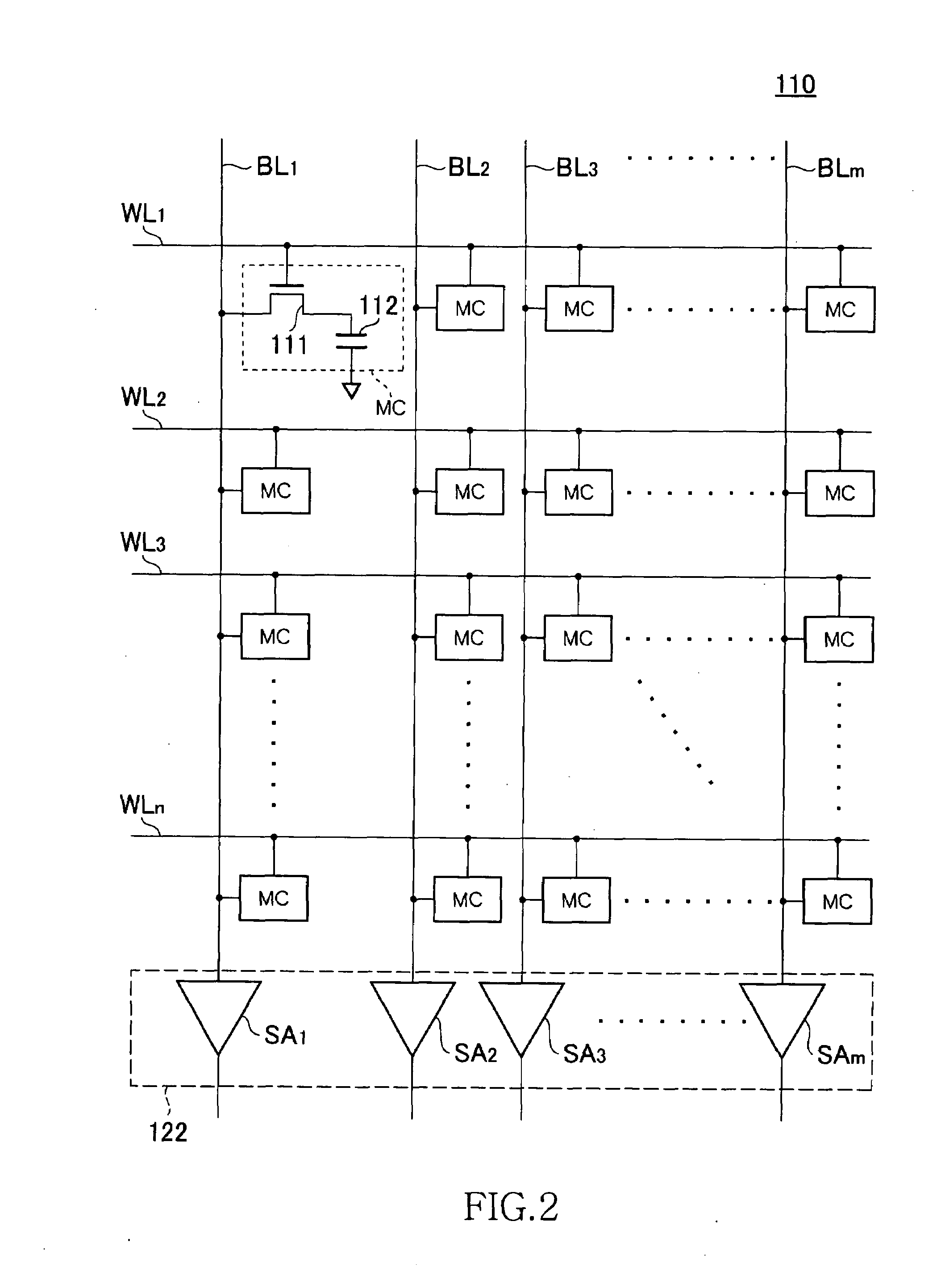
[0039]FIG. 2 is a circuit diagram schematically showing the configuration of the memory cell array 110.

[0040]As shown in FIG. 2, the memory cell array 110 has a matrix structure having plural word lines WL1 to WLn crossed with plural bit lines BL1 to BLm, and has a memory cell MC located at each intersection. Each memory cell MC includes a series circuit of a MOS transistor 111 and a capacitor 112. A drain of the MOS transistor 111 is connected to the corresponding bit lines BL1 to BLm, and a gate of ...

second embodiment

[0076]FIG. 9 is a block diagram showing a configuration of a semiconductor memory device 200 according to the

[0077]The semiconductor memory device 200 according to the second embodiment is different from the semiconductor memory device 100 according to the first embodiment in that the refresh cycle changing circuit 142 is replaced by a refresh cycle changing circuit 240. In other points, the semiconductor memory device 200 according to the second embodiment is the same as the semiconductor memory device 100 according to the first embodiment. Therefore, constituent elements that are the same as those in the first embodiment are denoted by like reference letters and numerals, and redundant explanations thereof will be omitted.

[0078]FIG. 10 is a block diagram showing a configuration of the refresh cycle changing circuit 240.

[0079]As shown in FIG. 10, the refresh cycle changing circuit 240 includes an address memory circuit 241 and a comparator circuit 242. The address memory circuit 24...

third embodiment

[0087]FIG. 12 is a block diagram showing a configuration of a semiconductor memory device 300 according to the present invention.

[0088]The semiconductor memory device 300 according to the third embodiment is different from the semiconductor memory device 100 according to the first embodiment in that the refresh cycle changing circuit 142 is replaced by a refresh cycle changing circuit 340. In other points, the semiconductor memory device 300 according to the third embodiment is the same as the semiconductor memory device 100 according to the first embodiment. Therefore, constituent elements that are the same as those in the first embodiment are denoted by like reference letters or numerals, and redundant explanations thereof will be omitted.

[0089]The refresh cycle changing circuit 340 generates a refresh cycle set signal RC3 including a digital value or an analog value of plural bits. While a detailed circuit configuration is not shown, a circuit including fuse elements correspondin...


PUM


Abstract

A semiconductor memory device includes a first refresh cycle changing circuit that changes a refresh cycle according to an auto-refresh mode, without giving influence to a refresh cycle according to a self-refresh mode, and a second refresh cycle changing circuit that changes a refresh cycle according to the self-refresh mode, without giving influence to a refresh cycle according to the auto-refresh mode. In this way, according to the present invention, the refresh cycle according to the auto-refresh mode and the refresh cycle according to the self-refresh mode can be controlled independently. Therefore, refresh operation considering the characteristic of each mode can be executed.

Description

TECHNICAL FIELD[0001]The present invention relates to a semiconductor memory device, and, more particularly to a semiconductor memory device requiring a refresh operation like a DRAM (Dynamic Random Access Memory).BACKGROUND OF THE INVENTION[0002]Among various semiconductor memory devices, a DRAM is one of the semiconductor memory devices most suitable for a large density, and is widely used for a main memory and the like of a computer. A prime reason that the DRAM is excellent for a large density is that a memory configuration of the DRAM is remarkably simple as compared with those of other semiconductor memory devices. In other words, each of memory cells of the DRAM includes one capacitor and one MOS transistor, and stores information based on a charge amount stored in the capacitor. Charging to and discharging from the capacitor are controlled by the MOS transistor connected to word lines. When the MOS transistor is turned on, a storage node of the capacitor is connected to a co...

Claims


Application Information

Patent Timeline
Patent Type & Authority Applications(United States)
IPC IPC(8): G11C11/406
CPCG11C11/406G11C11/40615G11C11/40611
Inventor DONO, CHIAKIKOSHIKAWA, YASUJI
Owner LONGITUDE LICENSING LTD
Why Eureka
Try Eureka