
Eureka
For R&D, Eureka makes reading and utilizing patents & technical documents easy.
Eureka AIR
Designed for self-driven R&D workflows. Generate viable solutions, solve complex R&D challenges, empower your innovation with AI.

Eureka Materials
Designed for material experts only. Revolutionize your material R&D, from search, analyze, to developing new materials.

TechResearch
Generate reliable direction feasibility study reports for your R&D in just a few steps.

TechSeek
Discover and master advanced knowledge NOW. Basics, ideas, possibilities, all at once.

TechMind
As an expert in R&D Theories, TechMind can generates customized viable solutions instantly.

TechRisk
Analyze your overall solution with one click, know your potential R&D risks in advance.

TechMonitor
Get weekly tech updates, stay abreast of the latest tech innovations and key insights.
Method of adjusting buried resistor resistance
- Summary
- Abstract
- Description
- Claims
- Application Information
AI Technical Summary
Benefits of technology
Problems solved by technology
Method used
Image

Examples
Embodiment Construction
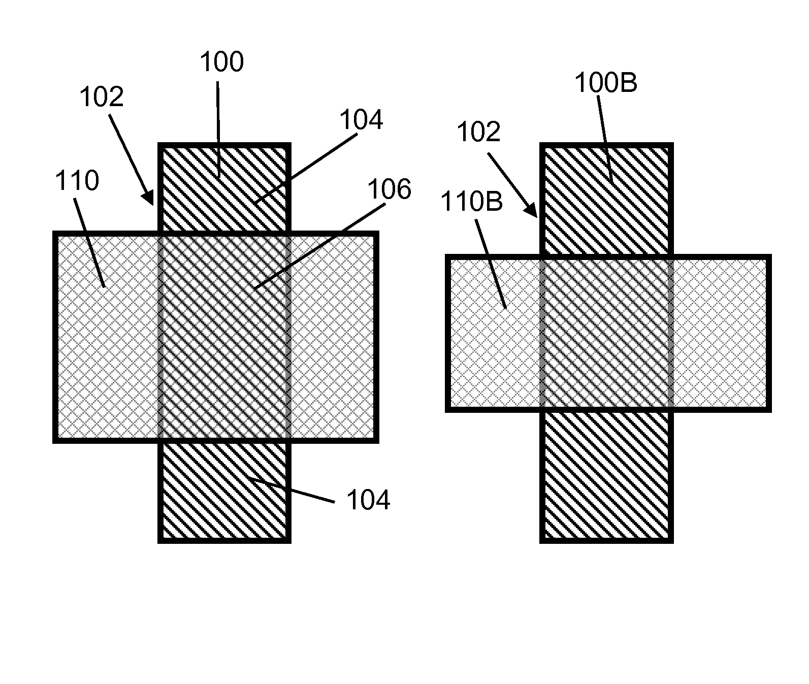
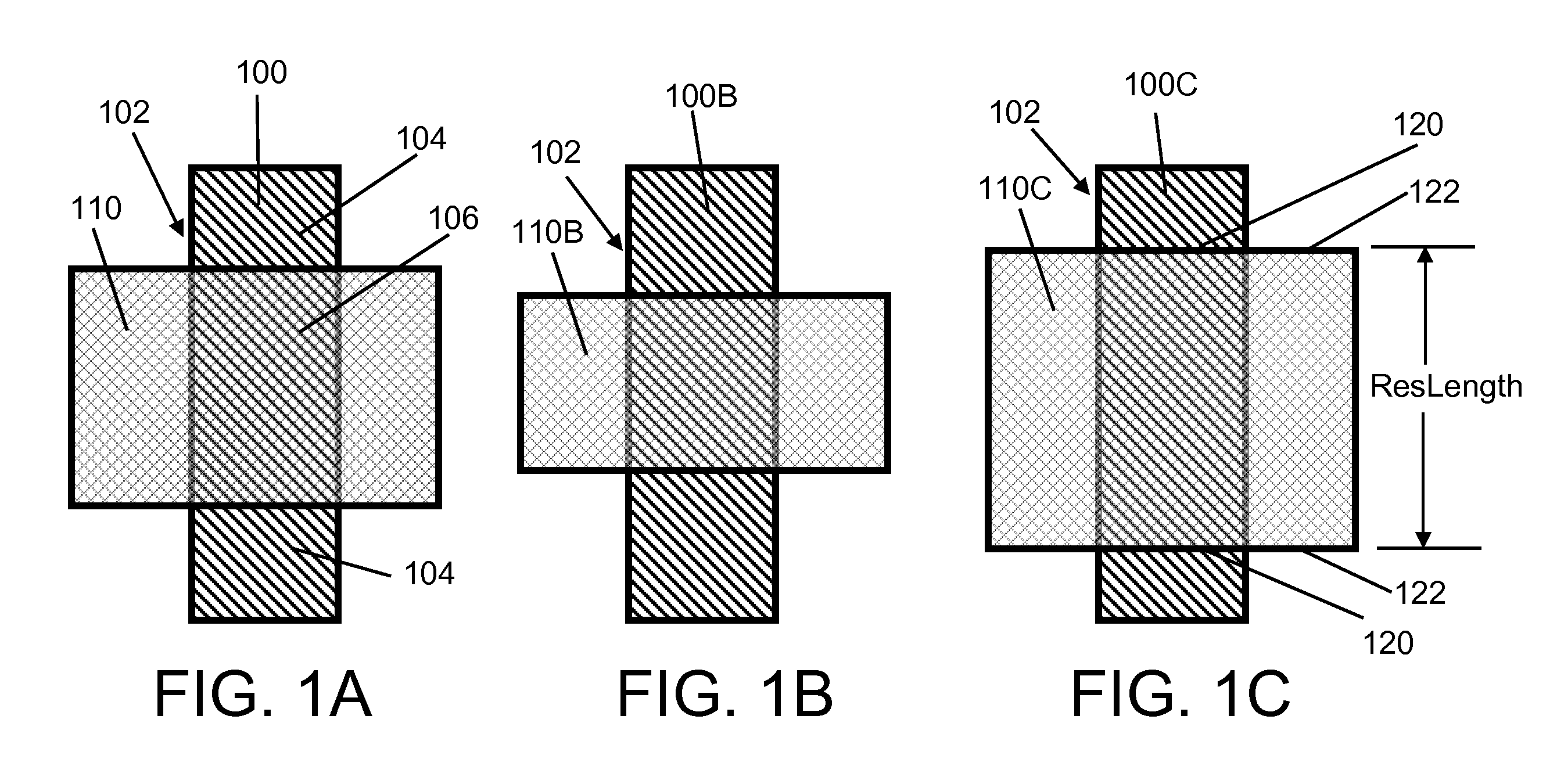
[0010]Referring to FIGS. 1A-1C, one embodiment of a method of adjusting the resistance of a buried resistor 100 is illustrated. In one embodiment, buried resistor 100 is an OP resistor formed in a semiconductor 102 (including 104 and 106, collectively). However, the teachings of the invention are applicable to other types of buried resistors. Semiconductor 102 may be either a polyconductor such as polysilicon or an active region of monocrystalline silicon.
[0011]In FIG. 1A, a silicidation blocking mask 110 is used to define buried resistor 100 in semiconductor 102. Silicidation blocking mask 110 may include, for example, one or more of silicon nitride, silicon dioxide and silicon oxy-nitride. Silicidation blocking mask 110 may be formed at any number of stages, for example, during formation of spacers (not shown) for FETs. At this stage, according to one embodiment, semiconductor 102 already has any implanting present necessary to generate its core film resistance value. Buried resis...
PUM
 Abstract
Description
Claims
Application Information
 - R&D Engineer
- R&D Manager
- IP Professional
- Industry Leading Data Capabilities
- Powerful AI technology
- Patent DNA Extraction
Browse by: Latest US Patents, China's latest patents, Technical Efficacy Thesaurus, Application Domain, Technology Topic, Popular Technical Reports.
© 2024 PatSnap. All rights reserved.Legal|Privacy policy|Modern Slavery Act Transparency Statement|Sitemap|About US| Contact US: help@patsnap.com