Method for manufacturing semiconductor device

a manufacturing method and semiconductor technology, applied in semiconductor devices, instruments, electrical equipment, etc., can solve the problems of destroying semiconductor elements, deteriorating semiconductors or insulators, and not showing expected characteristics, so as to prevent the increase of potential, reduce the electrical resistance of the surface, and reduce the electrical resistance

Active Publication Date: 2008-06-05
SEMICON ENERGY LAB CO LTD
View PDF65 Cites 80 Cited by
  • Summary
  • Abstract
  • Description
  • Claims
  • Application Information

AI Technical Summary

Benefits of technology

[0017]One object of the present invention is to avoid destruction and characteristic deterioration of a semiconductor element due to electric charge generated by peeling. In addition, in Reference 3, although a lower surface of a semiconductor element after peeling is limited to a conductive film, another object of the present invention is to permit us to select a high-resistant insulating material for a surface of the semiconductor element side after peeling.
[0027]Discharge is a phenomenon in which a current instantaneously flows to a portion where a current does not flow normally, such as an insulator or a semiconductor, due to a high potential difference. By wetting or moistening a surface which appears by peeling, electrical resistance of the surface can be reduced. As a result of decreasing electrical resistance, electric charge which is generated by peeling electrification diffuses on the wetted surface; therefore, a potential can be prevented from being increased as a potential of the surface which appears by peeling generates discharge. That is, according to the present invention, discharge due to peeling electrification can be prevented.
[0028]According to the present invention, since discharge due to peeling electrification is not generated, yield can be improved in a method for manufacturing the semiconductor device including a step of separating the substrate and the element formation layer. In addition, since characteristic deterioration of the semiconductor element due to the electrostatic breakdown can be eliminated, reliability of the semiconductor device can be improved according to the present invention.
[0029]In addition, electric charge generated by peeling cannot be discharged either inside of two separated layers by the method of the present invention. Therefore, even when a lower surface of the element formation layer is formed of an insulating material, the semiconductor element included in the element formation layer can be prevented from being destroyed by static electricity generated due to peeling electrification and characteristics of the semiconductor element can be prevented from being deteriorated.

Problems solved by technology

Even when the semiconductor element can operate without receiving damage which can be seen by appearance, a semiconductor or an insulator deteriorates due to high potential application and the semiconductor element does not show expected characteristics in some cases.
Therefore, when discharge due to static electricity is generated, there is a possibility that the semiconductor element can be destroyed, or the integrated circuit itself using the semiconductor element cannot be operated normally due to characteristic deterioration.
The electrostatic breakdown is one of causes which greatly reduce yield.
However, since discharge due to peeling electrification is an instantaneous event in which two layers are separated, elimination of electric charge by the ionizer is not in time in some cases.
However, in peeling electrification, since the surfaces of two layers to be separated are charged, the pass of discharge does not always pass through the protection circuit.
Accordingly, in peeling electrification, the electrostatic breakdown is not sufficiently prevented by the protection circuit.
Depending on an intended purpose of the stack, the conductive film becomes an obstacle and an expected intended purpose cannot be carried out because of the conductive film in some cases.

Method used


Image

  • Method for  manufacturing semiconductor device
  • Method for  manufacturing semiconductor device
  • Method for  manufacturing semiconductor device

Examples


example 1

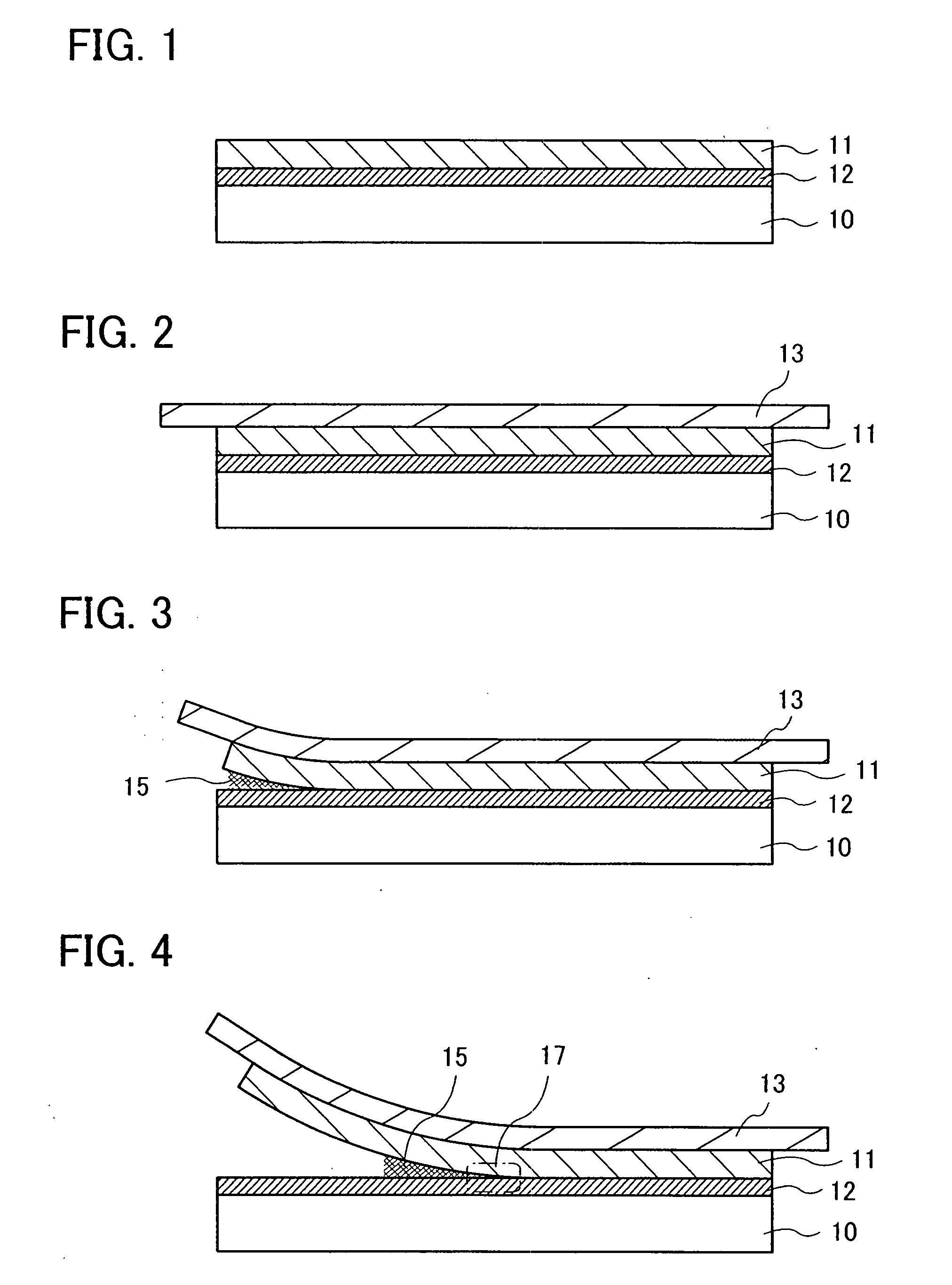
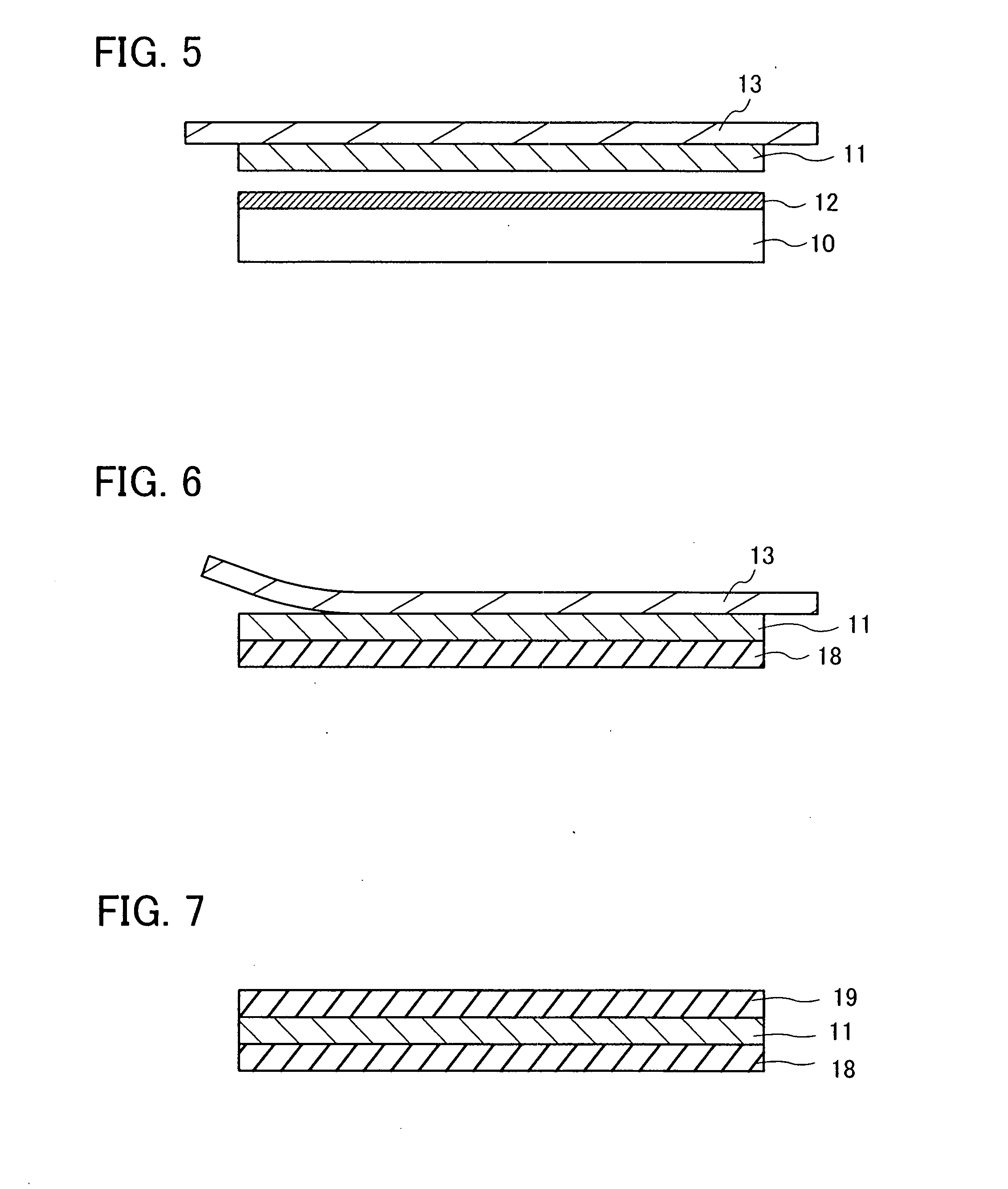
[0103]In this example, a method for manufacturing a semiconductor device capable of inputting and outputting data by noncontact, to which the present invention is applied, will be described. In this example, an element formation layer was provided with an integrated circuit which performs wireless communication using a 13.56 MHz signal and functions as an IC tag. This example will be described with reference to FIGS. 10 to 20, and 25 to 28.

[0104]As shown in FIG. 10, the release layer 101 was formed over the substrate 100, and an integrated circuit was formed over the release layer 101. A method for manufacturing the release layer 101 and the element formation layer 102 will be described with reference to FIGS. 25 to 28.

[0105]As the substrate 100, a substrate in which a glass substrate (a thickness of 0.7 mm, product name: AN100) made by Asahi Glass Co., Ltd. was cut to 5 inches on each side was used. As shown in FIG. 25, the release layer 101 had a multi-layer structure of a silicon...

example 2

[0132]In this example, a method for supplying the liquid 116, which is different from that described in Example 1, will be described. In this example, a method for spraying the liquid 116 in an atomized form is described and description of a common portion to that in Example 1 is omitted.

[0133]Similarly to Example 1, steps which have been described with reference to

[0134]FIGS. 10 to 13 are performed. Next, in Example 1, the plastic tweezers were inserted into the peeled lower surface of the element formation layer 102, and the gap 115 was generated between the upper surface of the release layer 101 and the lower surface of the element formation layer 102, as shown in FIG. 14. In this example, this step is unnecessary.

[0135]Next, the roller 118 is rolled on the heat release film 111 similarly to Example 1, and the element formation layer 102 with the heat release film 111 is peeled from the release layer 101. When the roller 118 is rolled, the liquid 116 in an atomized form was spray...

example 3

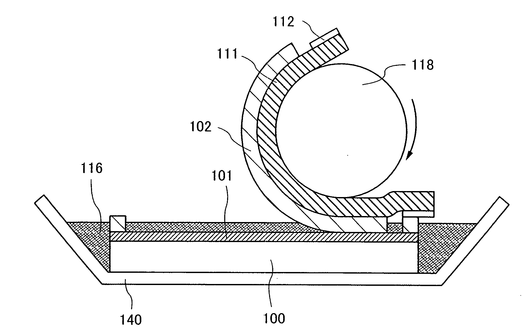
[0141]In this example, a method for supplying the liquid 116, which is different from those described in Example 1 and Example 2, will be described. Description of a common portion to that in Example 1 is omitted. In this example, a method for supplying liquid by separating the element formation layer 102 from a substrate while the substrate is being immersed in the liquid 116 is described.

[0142]Similarly to Example 1, steps described with reference to FIGS. 10 to 14 are performed. Next, as shown in FIG. 23, a container 140 which contains the liquid 116 is prepared. In the container 140, the substrate 100, the release layer 101, and the element formation layer 102 are immersed in the liquid 116. The substrate 100 is put in the container 140 so that the heat release film 111 comes on the top.

[0143]In this state, as shown in FIG. 24, the roller 118 is rolled on the heat release film 111, and the element formation layer 102 with the heat release film 111 is peeled from the release laye...


PUM

PropertyMeasurementUnit
temperatureaaaaaaaaaa
thicknessaaaaaaaaaa
resistivityaaaaaaaaaa

Abstract

An object is to suppress discharge due to static electricity generated by peeling, when an element formation layer including a semiconductor element is peeled from a substrate. Over the substrate, the release layer and the element formation layer are formed. The support base material which can be peeled later is fixed to the upper surface of the element formation layer. The element formation layer is transformed through the support base material, and peeling is generated at an interface between the element formation layer and the release layer. Peeling is performed while the liquid is being supplied so that the element formation layer and the release layer which appear sequentially by peeling are wetted with the liquid such as pure water. Electric charge generated on the surfaces of the element formation layer and the release layer can be diffused by the liquid, and discharge by peeling electrification can be eliminated.

Description

BACKGROUND OF THE INVENTION[0001]1. Field of the Invention[0002]The present invention relates to a method for manufacturing a semiconductor device, and relates to a technique for separating an element formation layer including a semiconductor element from a substrate which is used at the time of manufacture.[0003]In the present invention, a semiconductor device to be an object of manufacture includes a semiconductor element which can function by using semiconductor characteristics and general devices which function by using a plurality of semiconductor elements.[0004]As the semiconductor element, a MOS transistor, a transistor such as a thin film transistor, a diode, a MOS capacitor, and the like are given as examples. In addition, the semiconductor device includes an integrated circuit having a plurality of semiconductor elements, a device having a plurality of integrated circuits, or a device having an integrated circuit and another element. The integrated circuit includes a memor...

Claims


Application Information

Patent Timeline
Patent Type & Authority Applications(United States)
IPC IPC(8): H01L21/00G02F1/1368H01L21/02H01L27/12
CPCH01L21/67092H01L21/67132H01L27/1266H01L21/02252H01L21/707H01L21/02244G02F1/1333H01L21/77H01L21/78H01L21/7806H01L21/84H01L21/02315H01L21/02614H01L21/28202H01L21/76251H01L21/76259H01L27/12H01L27/1203
Inventor EGUCHI, SHINGOMONMA, YOHEITANI, ATSUHIROHIROSUE, MISAKOHASHIMOTO, KENICHIHOSAKA, YASUHARU
Owner SEMICON ENERGY LAB CO LTD
Why Eureka
Try Eureka