
Method for fabricating semiconductor device with recess gate

Active Publication Date: 2008-06-05
SK HYNIX INC
View PDF19 Cites 7 Cited by
  • Summary
  • Abstract
  • Description
  • Claims
  • Application Information

AI Technical Summary

Benefits of technology

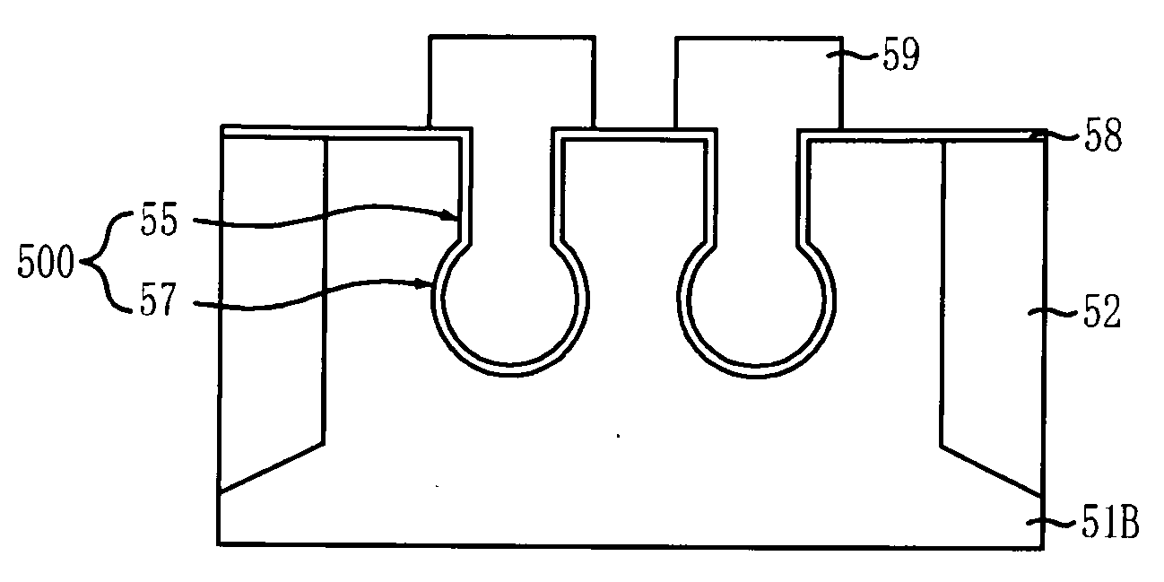
[0015]The present invention provides a method for fabricating a semiconductor device, and more particularly, a method for fabricating a recess gate in the semiconductor device, thereby improving thickness controllability and increasing process time for an oxide layer used as a passivation layer to form a bulb-type recess region. The method for fabricating the recess gate in the semiconductor device according to the present invention can also prevent deterioration of refresh characteristics of the semiconductor device caused by a seam which is formed in a gate electrode due to an extensive difference between a critical dimension (CD) of a first recess and that of a second recess for the bulb-type recess region and moves to an interface between a gate oxide layer and the gate electrode during a subsequent thermal process.

Problems solved by technology

Furthermore, as an ion implantation doping concentration to a substrate increases, junction leakage also increases due to an increasing electric field.
Thus, it may be difficult to secure refresh characteristics of a semiconductor device with a typical planar type transistor structure.
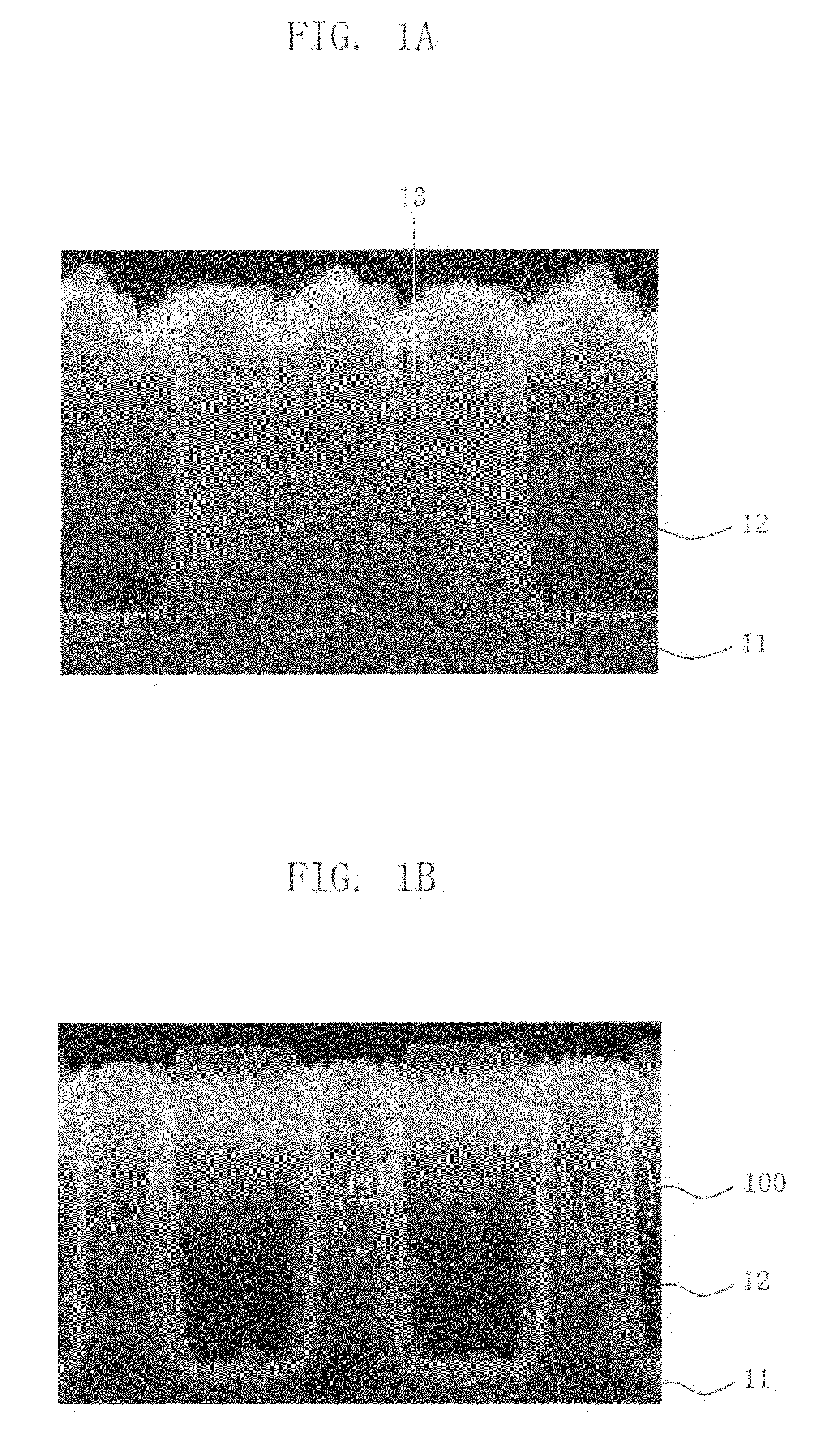
Since the horn 100 may become a source of leakage current, the refresh characteristics of the semiconductor device may be deteriorated.
When the thermal oxide layer is formed as the passivation layer, it requires a process time more than 5 hours and it is difficult to control a thickness of the thermal oxide layer.
Furthermore, when the passivation layer is formed by using the thermal oxide layer, a thickness of the passivation layer on the bottom portion of the first recess may be greater than that on the sidewalls of the first recess, in which case the second recess may not be formed if an etching target thickness of the subsequent etching process is not sufficient to break through the thick oxide layer on the bottom of the first recess.
Since the second recess is formed by an isotropic etching, it is difficult to control a CD of the second recess.
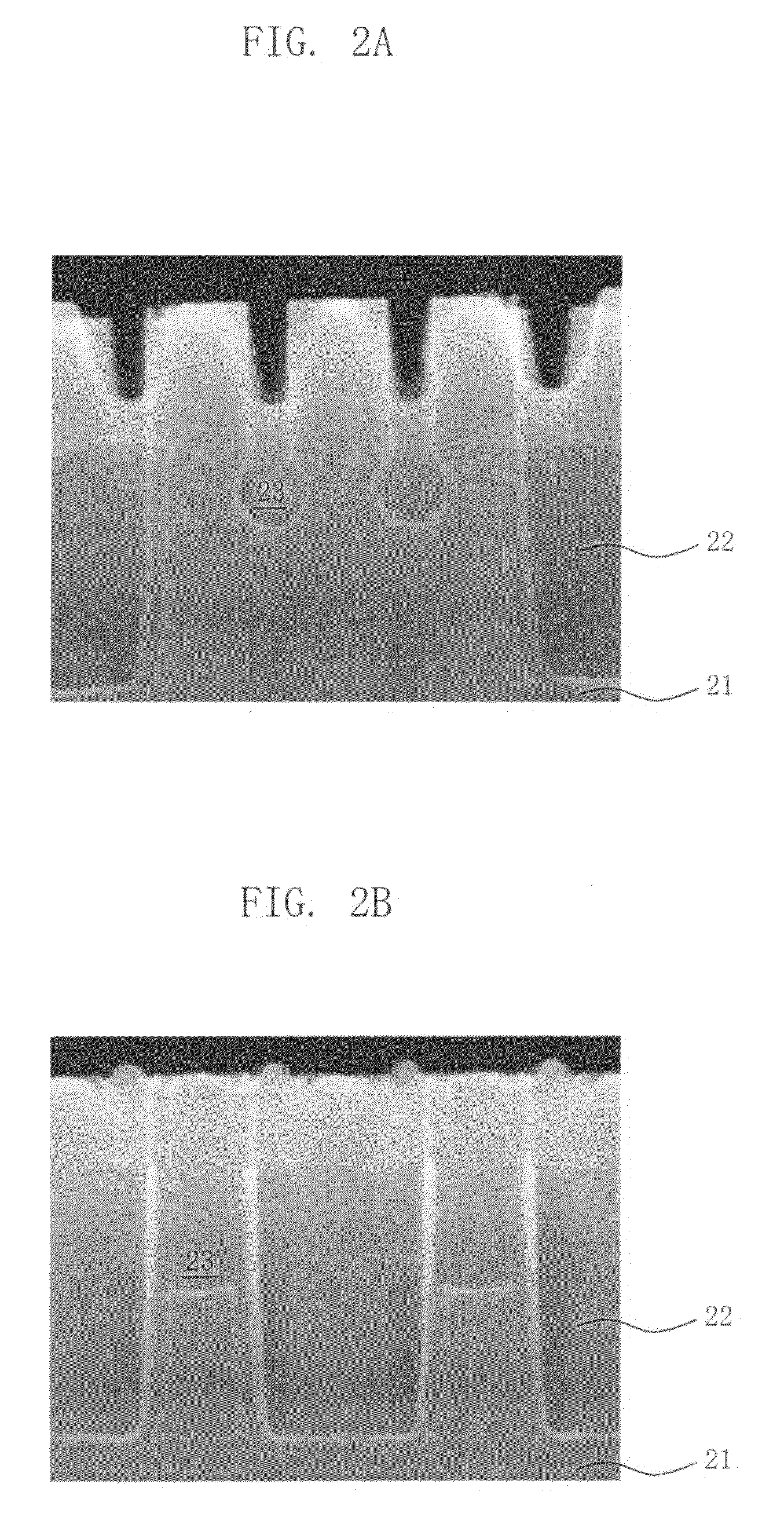
And in case that a thermal oxide layer is used as the passivation layer, it becomes more difficult to control the CD of the second recess due to non-uniform thickness of the thermal oxide layer, which may cause unwanted increase in the CD of the second recess.

Method used


Image

  • Method for fabricating semiconductor device with recess gate
  • Method for fabricating semiconductor device with recess gate
  • Method for fabricating semiconductor device with recess gate

Examples


Embodiment Construction

[0022]FIGS. 5A to 5G illustrate cross-sectional views of a method for fabricating a transistor with a recess gate in accordance with an embodiment of the present invention.

[0023]Referring to FIG. 5A, an isolation layer 52 is formed in a substrate 51 to define an active region. The substrate 51 is selectively etched to form a trench and an insulation layer is formed to fill the trench. The insulation layer is planarized to form the isolation layer 52. A sacrificial oxide layer and a hard mask are successively stacked over the substrate 51 and the isolation layer 52 and a photoresist pattern (not shown) is formed over the hard mask. The hard mask and the sacrificial oxide layer are successively etched by using the photoresist pattern as an etch mask. Thus, a first mask pattern 53 and a second mask pattern 54 are formed to define a recess target region over the substrate 51 and the isolation layer 52.

[0024]The first mask pattern 53 protects the substrate 51 from a top attack and can be...


PUM


Abstract

A method for fabricating a semiconductor device includes forming a first recess in a substrate, forming a plasma oxide layer over the substrate including first recess, etching the plasma oxide layer to have a portion of the plasma oxide layer remain on sidewalls of the first recess, and forming a second recess by isotropically etching a bottom portion of the first recess, wherein the second recess has a width greater than a width of the first recess.

Description

CROSS-REFERENCE TO RELATED APPLICATIONS[0001]The present invention claims priority of Korean patent application number 10-2006-0108820 filed on Nov. 6, 2006, which is incorporated by reference in its entirety.BACKGROUND OF THE INVENTION[0002]The present invention relates to a method for fabricating a semiconductor device, and more particularly, to a method for fabricating a semiconductor device including a recess gate.[0003]As semiconductor devices become highly integrated, a channel length of a memory cell transistor decreases. Furthermore, as an ion implantation doping concentration to a substrate increases, junction leakage also increases due to an increasing electric field. Thus, it may be difficult to secure refresh characteristics of a semiconductor device with a typical planar type transistor structure.[0004]Thus, a three-dimensional (3D) recess gate process has been introduced to overcome the above limitations. According to the process, a portion of an active region in a sub...

Claims


Application Information

Patent Timeline
IPC IPC(8): H01L21/311
CPCH01L29/66553H01L29/1037H01L27/10876H01L29/66621H10B12/053H01L21/18
Inventor KIM, MYUNG-OK
Owner SK HYNIX INC
Learn More