Method for manufacturing semiconductor device and semiconductor device

a semiconductor device and semiconductor technology, applied in semiconductor devices, semiconductor/solid-state device details, electrical apparatus, etc., can solve problems such as power supply and transmission speed problems, wafer cracking, and failure to achieve desired element characteristics in some cases, so as to prevent substrate cracking and improve workability and productivity.

Active Publication Date: 2008-06-12
SONY CORP
View PDF7 Cites 35 Cited by
  • Summary
  • Abstract
  • Description
  • Claims
  • Application Information

AI Technical Summary

Benefits of technology

[0017]It is desirable to provide a method for manufacturing a semiconductor device which is capable of decreasing the influence of a difference in thermal expansion between a semiconductor substrate and a buried conductor layer and forming desired via holes without the need for high alignment accuracy and ultra thinning of a wafer.
[0030]As described above, according to the present invention, a via structure capable of preventing substrate cracking due to a difference in thermal expansion between a buried conductor layer and a semiconductor substrate can be stably formed without degrading workability and productivity.

Problems solved by technology

However, in the first via forming method in which the bottom of a buried conductor layer is exposed by grinding the back side of a wafer, a via hole is entirely composed of the buried conductor layer to cause a limitation of the constituent material of the conductor layer buried in the wafer, thereby failing to achieve desired element characteristics in some cases.
However, the thermal expansion coefficients of Cu and W greatly differ from that of Si (silicon) constituting the wafer, and thus the wafer is likely to be cracked during heating in a subsequent element forming step.
In this case, however, it is difficult to form low-resistance via holes, leaving problems with power supply and transmission speed.
However, when the wafer becomes ultrathin, the element characteristics may be changed or handleability may be decreased to degrade productivity.
However, the limit of the accuracy of alignment from the back side of the wafer is 0.5 μm and thus does not reach a necessary spec.
Therefore, when the contact hole is formed by a photolithographic technique, there is the problem that a mask pattern cannot be formed with required alignment accuracy, and it is difficult to cause the wiring layer to function as a sufficient etching stopper in processing because of its small thickness.
As described above, when the wafer is ultra-thinned, handleability of the wafer in a subsequent step is decreased to degrade productivity.

Method used


Image

  • Method for manufacturing semiconductor device and semiconductor device
  • Method for manufacturing semiconductor device and semiconductor device
  • Method for manufacturing semiconductor device and semiconductor device

Examples


first embodiment

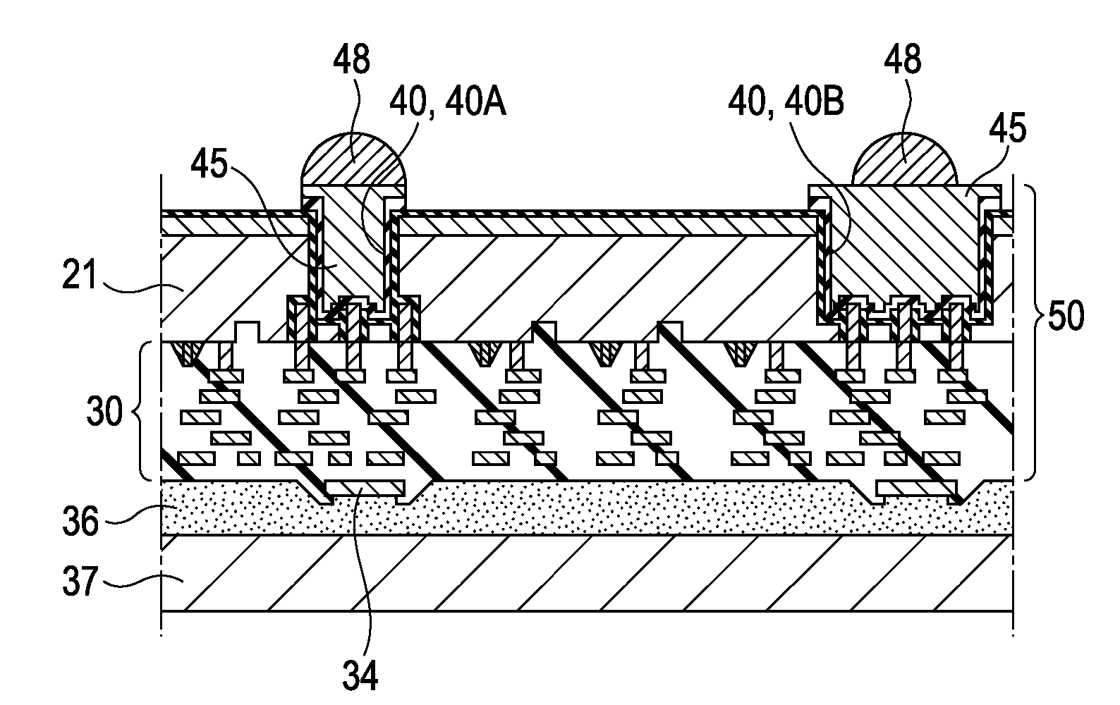
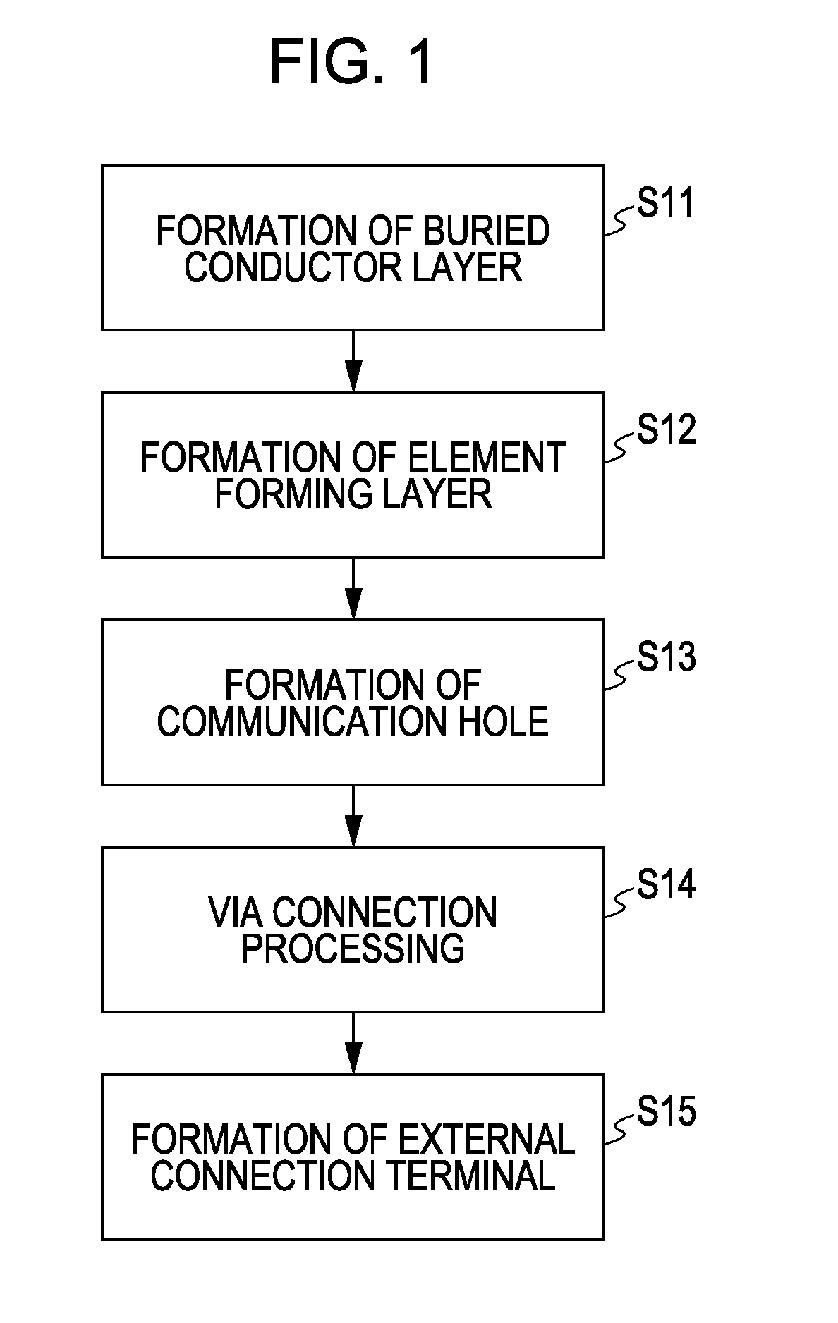
[0049]FIG. 1 is a flowchart illustrating a method for manufacturing a semiconductor device according to a first embodiment of the present invention. The method for manufacturing a semiconductor device of this embodiment includes the steps of forming buried conductor layers on one (first surface) of the surfaces of a semiconductor substrate (S11), forming an element forming layer including semiconductor elements such as transistors, wiring, various insulating layers, electrode pads, etc. on the first surface of the semiconductor substrate (S12), forming communication holes in the other surface (second surface) of the semiconductor substrate so that the communication holes communicate with the buried conductor layers (S13), electrically connecting the buried conductor layers and the communication holes (S14), and forming external connection terminals on the second surface of the semiconductor substrate (S15).

Step of Forming Buried Conductor Layer

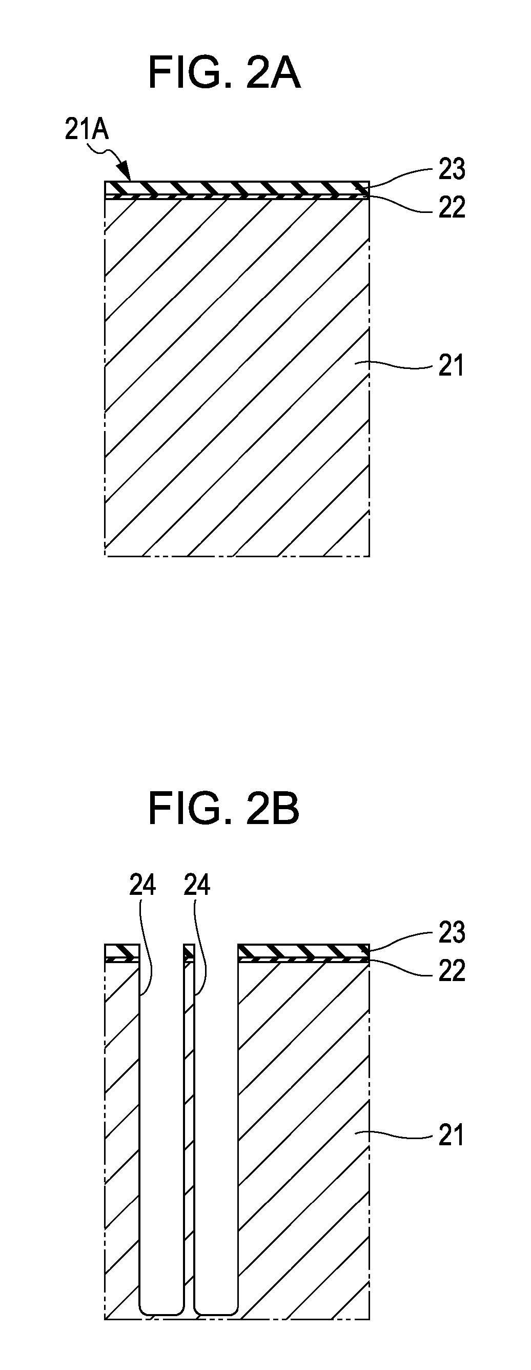
[0050]FIGS. 2A, 2B, and 3C to 3E are se...

second embodiment

[0087]FIG. 11 is a flowchart illustrating a method for manufacturing a semiconductor device according to a second embodiment of the present invention. The method for manufacturing a semiconductor device of this embodiment includes the steps of forming an element forming layer on a first surface of a semiconductor substrate (S21), forming buried conductor layers on the first surface of the semiconductor substrate through the element forming layer (S22), forming communication holes in the second surface of the semiconductor substrate so that the communication holes communicate with the buried conductor layers (S23), electrically connecting the buried conductor layers and the communication holes (S24), and forming external connection terminals on the second surface of the semiconductor substrate (S25).

[0088]In other words, in the first embodiment, the step of forming buried conductor layers is performed before the step of forming an element forming layer. However, this embodiment is di...


PUM


Abstract

A method for manufacturing a semiconductor device includes the steps of providing an element forming layer on a first surface of a semiconductor substrate, and providing an external connection terminal on a second surface of the semiconductor substrate opposite to the first surface so that the external connection terminal is electrically connected to the element forming layer through a via hole. The via hole is formed through the steps of forming a buried conductor layer on the first surface so as to electrically insulate the buried conductor layer from the semiconductor substrate, forming a communication hole on the second surface so as to communicate it with the buried conductor layer, and electrically connecting the buried conductor layer and the communication hole.

Description

CROSS REFERENCES TO RELATED APPLICATIONS[0001]The present invention contains subject matter related to Japanese Patent Application JP 2006-329179 filed in the Japanese Patent Office on Dec. 6, 2006, the entire contents of which are incorporated herein by reference.BACKGROUND OF THE INVENTION[0002]1. Field of the Invention[0003]The present invention relates to a method for manufacturing a semiconductor device including via holes passing through a semiconductor substrate and to a semiconductor device.[0004]2. Description of the Related Art[0005]Electronic components have recently been increased in integration density and mounting density accompanying the demand for improving the functions of electronic apparatuses and compacting them. Therefore, MCM (multi-chip module) or SIP (system-in package) type semiconductor devices using flip-chip mounting are becoming mainstream. Such semiconductor devices include a semiconductor device having a chip-on-chip (COC) structure in which a second s...

Claims


Application Information

Patent Timeline
Patent Type & Authority Applications(United States)
IPC IPC(8): H01L23/48H01L21/44
CPCH01L21/563H01L21/76898H01L23/481H01L24/12H01L25/0657H01L2224/0401H01L2224/13025H01L2224/13099H01L2224/16145H01L2224/16225H01L2224/48227H01L2224/73204H01L2224/73265H01L2924/01002H01L2924/01004H01L2924/01005H01L2924/01014H01L2924/01018H01L2924/01022H01L2924/01029H01L2924/01033H01L2924/0105H01L2924/01073H01L2924/01074H01L2924/01075H01L2924/01078H01L2924/01082H01L2924/014H01L2924/04953H01L2924/05042H01L2924/15311H01L2924/19043H01L24/48H01L2924/01006H01L2924/01023H01L2224/32225H01L2225/0651H01L2225/06517H01L2225/06513H01L2225/06541H01L2225/06568H01L2224/32145H01L2224/92125H01L2224/05572H01L2224/04042H01L24/05H01L2924/0002H01L2924/00H01L2924/00012H01L2224/05552H01L24/73H01L2224/11H01L2924/00014H01L2224/26175H01L2224/26145H01L2224/023H01L2224/45099H01L2224/45015H01L2924/207H01L2924/0001H01L23/48H01L23/12
Inventor KOMAI, NAOKINAKAMURA, TAKUYA
Owner SONY CORP
Why Eureka
Try Eureka