Substrate Polishing Apparatus And Substrate Polishing Method

a technology of substrate polishing and polishing apparatus, which is applied in the direction of lapping machines, instruments, manufacturing tools, etc., can solve the problems of increasing the size of semiconductor devices, increasing the complexity of semiconductor elements, and reducing the polishing effect, so as to achieve uniform and stable polishing results

Active Publication Date: 2008-06-12
EBARA CORP
View PDF4 Cites 45 Cited by
  • Summary
  • Abstract
  • Description
  • Claims
  • Application Information

AI Technical Summary

Benefits of technology

[0010]The present invention has been made in view of the above drawbacks. It is an object of the present invention to provide a substrate polishing apparatus and a substrate polishing method which can appropriately polish a substrate such as a semiconductor wafer according to a thickness distribution of a film formed on a surface of the substrate so as to obtain a uniform film thickness.
[0030]The substrate polishing apparatus according to the present invention has the substrate holder capable of adjusting the pressing forces distributed along the radial direction of the substrate and the film thickness measuring device capable of measuring the film thicknesses distributed along the radial direction. Therefore, the operation data (recipe) of the substrate holder can be automatically adjusted, and hence a uniform and stable polishing result can be achieved. Further, in a case of polishing a double-layer film comprising a Cu film and a barrier film of Ta or the like, for example, an interface between these two films can be detected by the film thickness measuring device, and hence the polishing conditions such as the pressing forces can be changed from those for the Cu film to those for the barrier film. The oscillation frequency of an oscillator of the eddy current sensor, for example, of the film thickness measuring device can be changed so as to place the film thickness measuring device itself under a condition suitable for detecting the barrier film.

Problems solved by technology

In recent years, semiconductor devices have become smaller in size and structures of semiconductor elements have become more complicated.
Accordingly, irregularities on a surface of a semiconductor device become increased, and hence step heights on the surface of the semiconductor device tend to be larger.
Further, an open circuit is caused by disconnection of interconnects, or a short circuit is caused by insufficient insulation between interconnect layers.
As a result, good products cannot be obtained, and the yield tends to be reduced.
Furthermore, even if a semiconductor device initially works normally, reliability of the semiconductor device is lowered after a long-term use.
Therefore, if the irregularities of the surface of the semiconductor device are increased, then it becomes difficult to form a fine pattern on the semiconductor device.
In such a polishing apparatus, if a relative pressing force between the semiconductor wafer being polished and the polishing surface of the polishing pad is not uniform over an entire surface of the semiconductor wafer, then the semiconductor wafer may insufficiently be polished or may excessively be polished at some portions depending on the pressing force applied to those portions of the semiconductor wafer.
The polishing pad is so elastic that the pressing force applied to a peripheral portion of the semiconductor wafer tends to become non-uniform.

Method used


Image

  • Substrate Polishing Apparatus And Substrate Polishing Method
  • Substrate Polishing Apparatus And Substrate Polishing Method
  • Substrate Polishing Apparatus And Substrate Polishing Method

Examples


Embodiment Construction

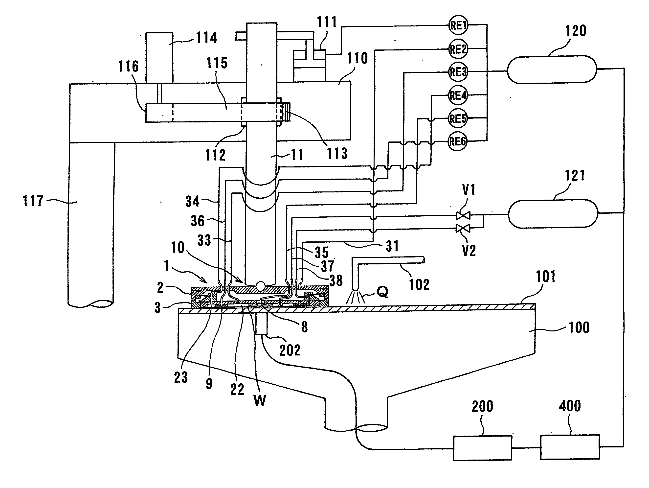
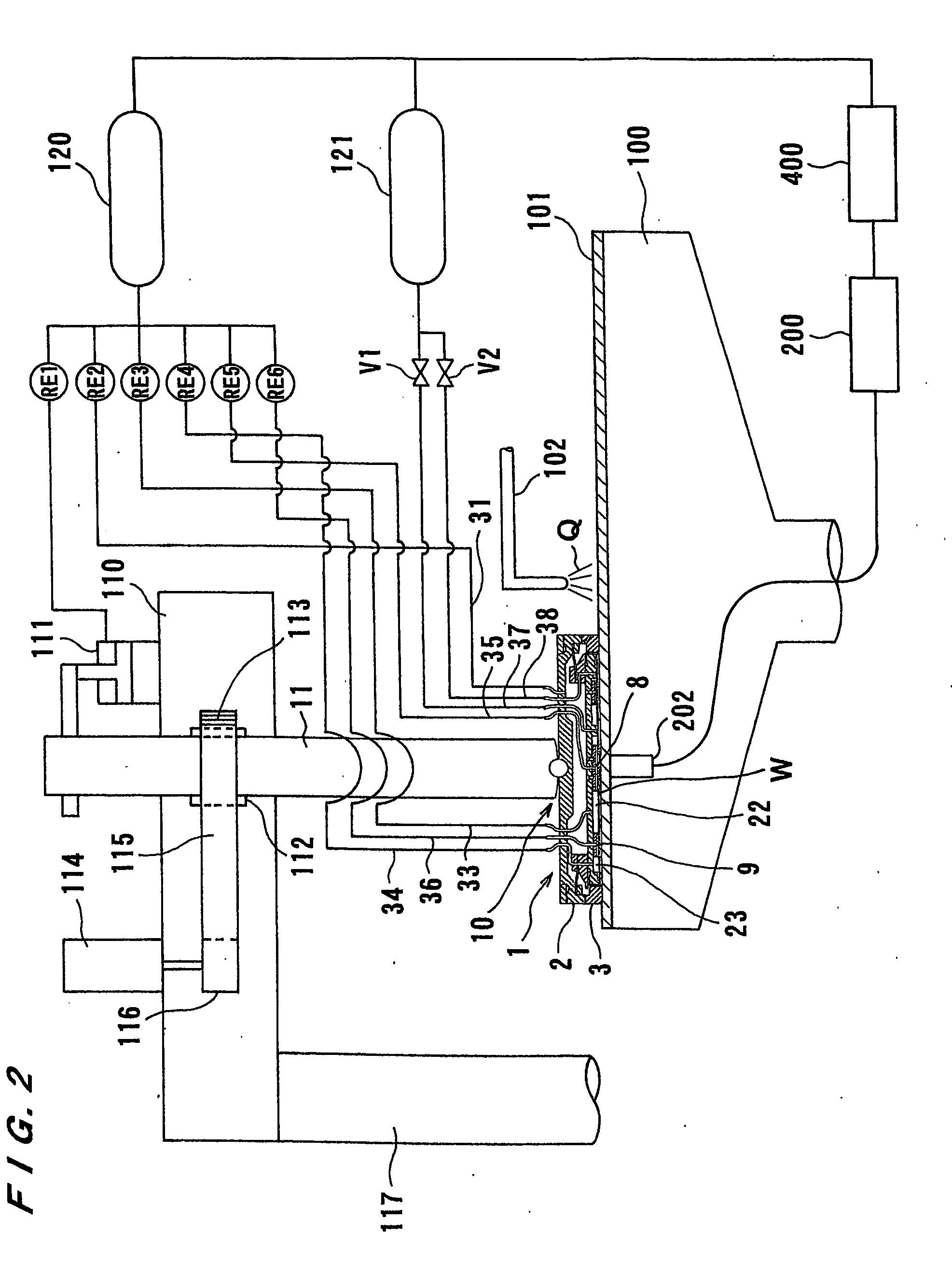
[0055]A substrate polishing apparatus and a substrate polishing method according to an embodiment of the present invention will be described below with reference to the accompanying drawings. FIGS. 1 through 24C show a substrate polishing apparatus which performs a substrate polishing method according to an embodiment of the present invention.

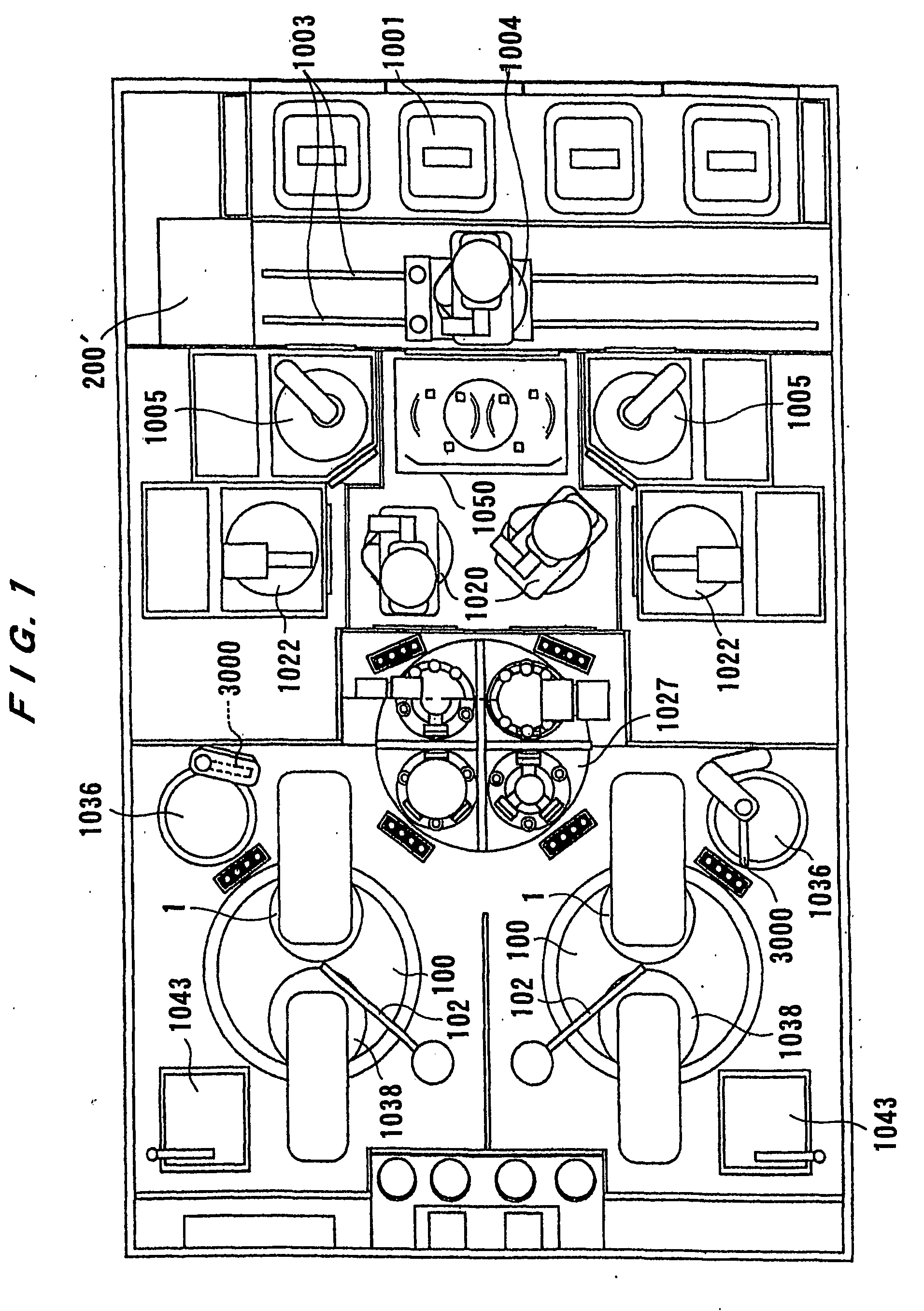
[0056]FIG. 1 is a plan view showing an arrangement of the substrate polishing apparatus according to the embodiment of the present invention. The substrate polishing apparatus comprises polishing tables 100 each having a polishing surface, top rings (substrate holders) 1 each for holding a substrate to be polished and pressing the substrate against the polishing surface, and a film thickness measuring device 200′ for measuring a thickness of a film formed on the substrate.

[0057]The substrate polishing apparatus comprises a transfer robot 1004 which is movable on rails 1003 for transferring a substrate such as a semiconductor wafer to and from c...


PUM

PropertyMeasurementUnit
thicknessaaaaaaaaaa
distanceaaaaaaaaaa
frequencyaaaaaaaaaa

Abstract

The present invention relates to a substrate polishing apparatus and a substrate polishing method for polishing a substrate such as a semiconductor wafer to a flat finish. The substrate polishing apparatus includes a polishing table (100) having a polishing surface (101), a substrate holder (1) for holding and pressing a substrate (W) against the polishing surface (101) of the polishing table (100), and a film thickness measuring device (200) for measuring a thickness of a film on the substrate (W). The substrate holder (1) has a plurality of pressure adjustable chambers (22 to 25), and pressures in the respective chambers (22 to 25) are adjusted based on the film thickness measured by the film thickness measuring device (200).

Description

TECHNICAL FIELD[0001]The present invention relates to a substrate polishing apparatus and a substrate polishing method for polishing a substrate such as a semiconductor wafer to a flat finish.BACKGROUND ART[0002]In recent years, semiconductor devices have become smaller in size and structures of semiconductor elements have become more complicated. In addition, the number of layers in multilayer interconnects used for a logical system has been increased. Accordingly, irregularities on a surface of a semiconductor device become increased, and hence step heights on the surface of the semiconductor device tend to be larger. This is because, in a manufacturing process of a semiconductor device, a thin film is formed on a semiconductor device, then micromachining processes, such as patterning or forming holes, are performed on the semiconductor device, and these processes are repeated many times to form subsequent thin films on the semiconductor device.[0003]When the number of irregularit...

Claims


Application Information

Patent Timeline
Patent Type & Authority Applications(United States)
IPC IPC(8): B24B49/04B24B29/02B24B37/005B24B37/013B24B37/30B24B37/32B24B49/10B24B49/12B24B49/16H01L21/304
CPCB24B37/013B24B49/16B24B49/12B24B49/105B24B37/00B24B37/04B24B49/00H01L21/304
Inventor TOGAWA, TETSUJIFUKAYA, KOICHITADA, MITSUOTAKAHASHI, TAROSUTO, YASUNARI
Owner EBARA CORP
Why Eureka
Try Eureka