Megasonic precision cleaning of semiconductor process equipment components and parts

a technology of semiconductor process equipment and parts, applied in the direction of cleaning process and equipment, cleaning process using liquids, chemistry apparatus and processes, etc., can solve the problems of affecting the yield of wafer fabrication lines and devices, the inability of low-frequency ultrasonic cleaning techniques to effectively remove submicron particles from processing parts, and the cross-contamination of trace metals between semiconductor wafers

Active Publication Date: 2008-06-19
LAM RES CORP
View PDF88 Cites 22 Cited by
  • Summary
  • Abstract
  • Description
  • Claims
  • Application Information

AI Technical Summary

Benefits of technology

[0007]In one embodiment, the present invention provides an apparatus for cleaning a processing component. The apparatus comprises a tank having a cavity defined by a based and one or more sidewalls extending therefrom and an opening opposite the base. The tank is configured to hold a volume of fluid within...

Problems solved by technology

However, there are persistent concerns regarding particulate and trace metal cross-contamination between semiconductor wafers, magnetic media and the parts, equipment, or tools, etc. that are used to process these semiconductor wafers, magnetic media.
However, as the critical dimensions of semiconductor wafers etc. continue to decrease and the number o...

Method used


Image

  • Megasonic precision cleaning of semiconductor process equipment components and parts
  • Megasonic precision cleaning of semiconductor process equipment components and parts
  • Megasonic precision cleaning of semiconductor process equipment components and parts

Examples


Embodiment Construction

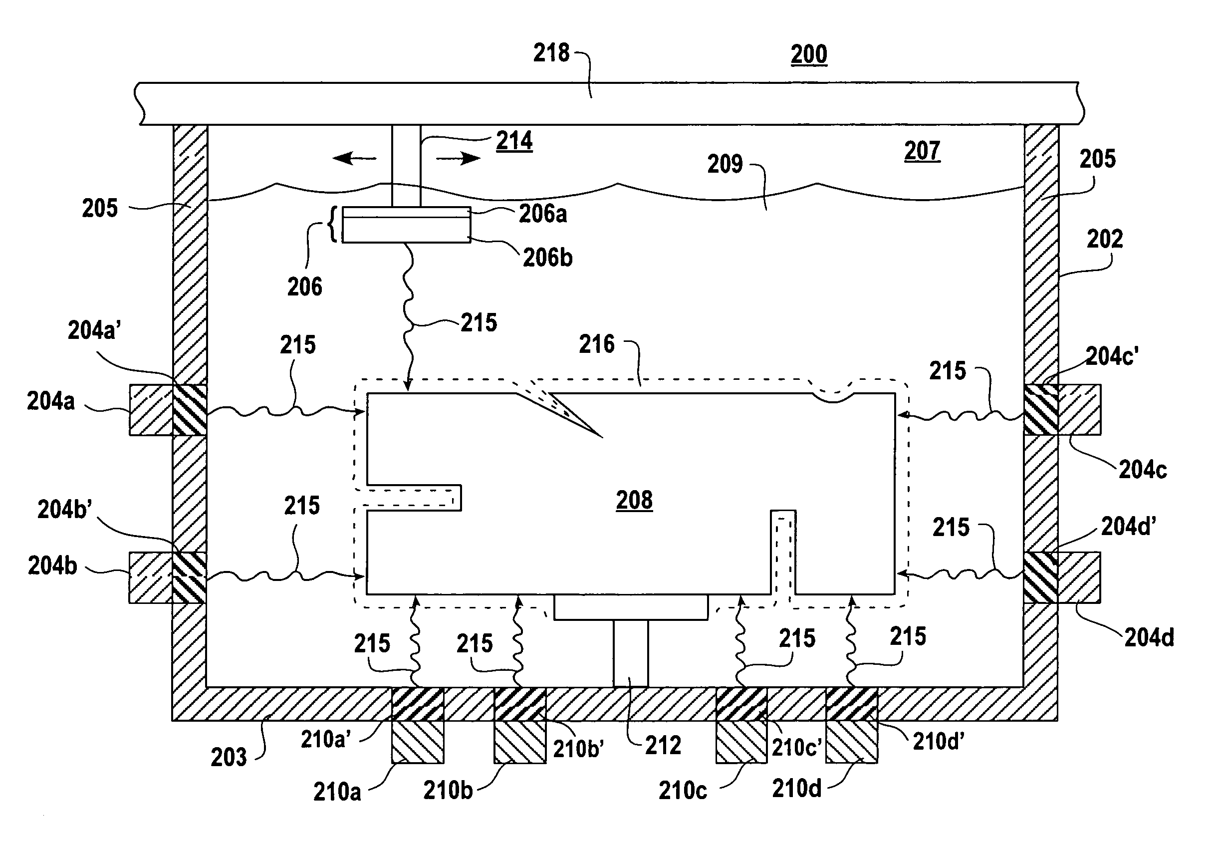
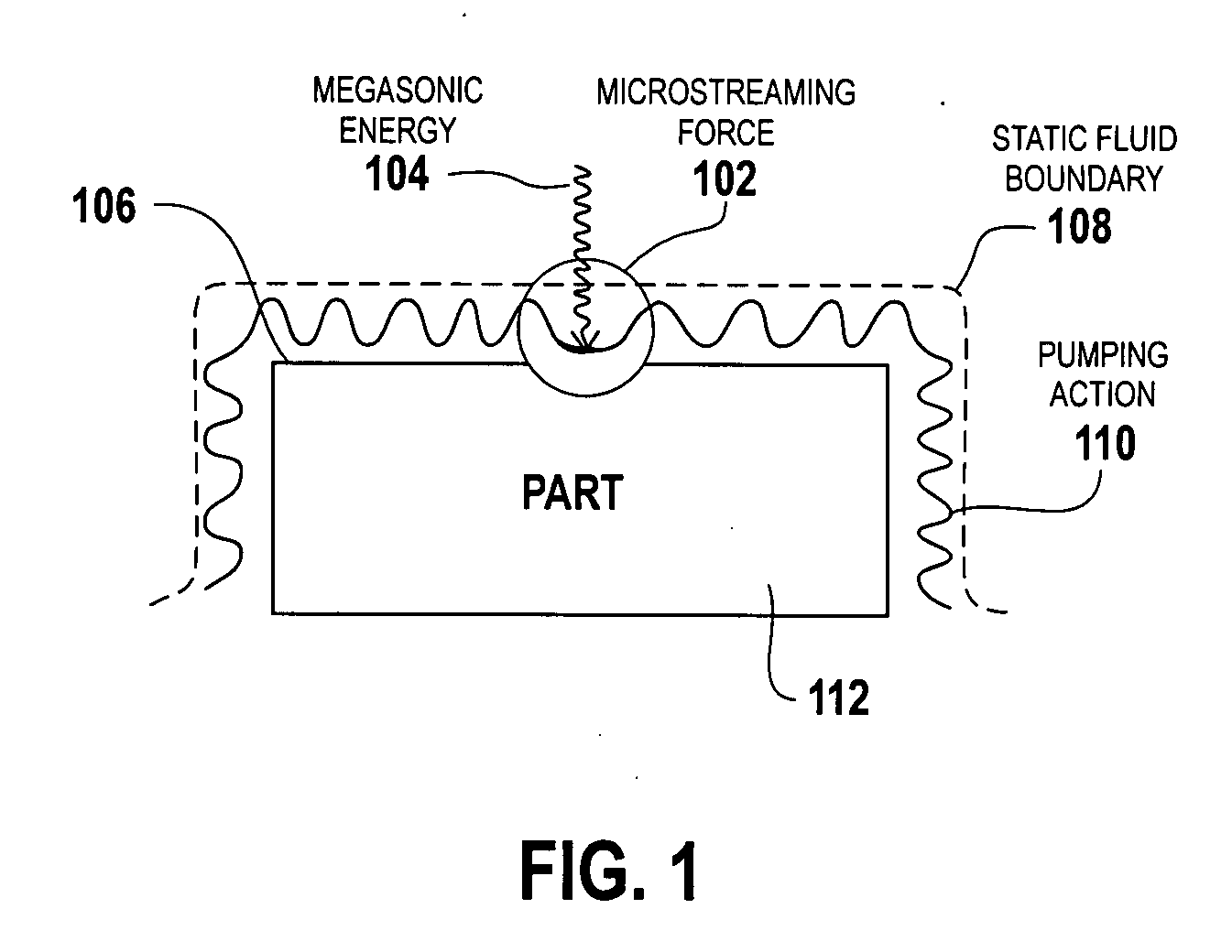
[0019]Embodiments of the present invention provide systems, apparatus, and methods for applying megasonic energy to effectively remove submicron particulate contamination from electronic device processing parts, components, tools, etc. or any other part, component, tool, etc. that is not a substrate or wafer, but that can be subject to inorganic or organic submicron particulate contamination. Specifically, embodiments of the present invention provide an approach for using high frequency megasonic energy (approximately 600 KHz-2 MHz) and selective cleaning media (e.g. chemicals, fluids, etc.) in conjunction with various precision cleaning apparatus to remove submicron particles from the surfaces and sidewalls of processing parts, components, tools, etc.

[0020]The precision cleaning apparatus of embodiments of the present invention can include megasonic tanks, scanning megasonic plates, megasonic jets, and megasonic sweeping beams that can be used to enhance micro-streaming forces (see...


PUM


Abstract

Methods and apparatus are provided for using various megasonic apparatus including megasonic tanks, scanning megasonic plates, megasonic jets, and megasonic sweeping beams etc., in combination with selective chemistries to remove sub-micron particulate contaminants from the surfaces of the processing equipment used in semiconductor, medical, or any other processing environments.

Description

BACKGROUND[0001]1. Field of the Invention[0002]The invention relates generally to the precision cleaning of processing and manufacturing equipment and, more particularly, to apparatus and methods for utilizing high frequency megasonic energy in combination with selective cleaning media to clean electronic device processing and manufacturing equipment, and other types of processing and manufacturing equipment etc.[0003]2. Description of the Related Art[0004]In electronic device manufacturing operations, megasonic cleaning is widely used to remove particle contamination from semiconductor wafers, magnetic media, etc. to mitigate against the detrimental effects of particle contamination on wafer yield and device reliability. However, there are persistent concerns regarding particulate and trace metal cross-contamination between semiconductor wafers, magnetic media and the parts, equipment, or tools, etc. that are used to process these semiconductor wafers, magnetic media.[0005]Conventi...

Claims


Application Information

Patent Timeline
IPC IPC(8): B08B3/12B08B3/02B08B3/04B08B3/08
CPCB08B3/12H01L21/67086H01L21/67057H01L21/67051B08B2203/0288H01L21/302
Inventor YIN, YAOBO
Owner LAM RES CORP
Why Eureka
Try Eureka