Dummy patterns and method of manufacture for mechanical strength of low k dielectric materials in copper interconnect structures for semiconductor devices

Active Publication Date: 2008-06-19
SEMICON MFG INT (SHANGHAI) CORP
View PDF3 Cites 14 Cited by
  • Summary
  • Abstract
  • Description
  • Claims
  • Application Information

AI Technical Summary

Benefits of technology

[0010]According to the present invention, techniques directed to integrated circuits and their processing for the manufacture of semiconductor devices are provided. In particular, the invention provides a method and structures for manufacturing bond pad structures for integrated circuit devices. More particularly, the invent

Problems solved by technology

Conventional semiconductor fabrication plants often costs hundreds of millions or even billions of U.S. dollars to construct.
Making devices smaller is always very challenging, as each process for the manufacture of

Method used


Image

  • Dummy patterns and method of manufacture for mechanical strength of low k dielectric materials in copper interconnect structures for semiconductor devices
  • Dummy patterns and method of manufacture for mechanical strength of low k dielectric materials in copper interconnect structures for semiconductor devices
  • Dummy patterns and method of manufacture for mechanical strength of low k dielectric materials in copper interconnect structures for semiconductor devices

Examples


Example

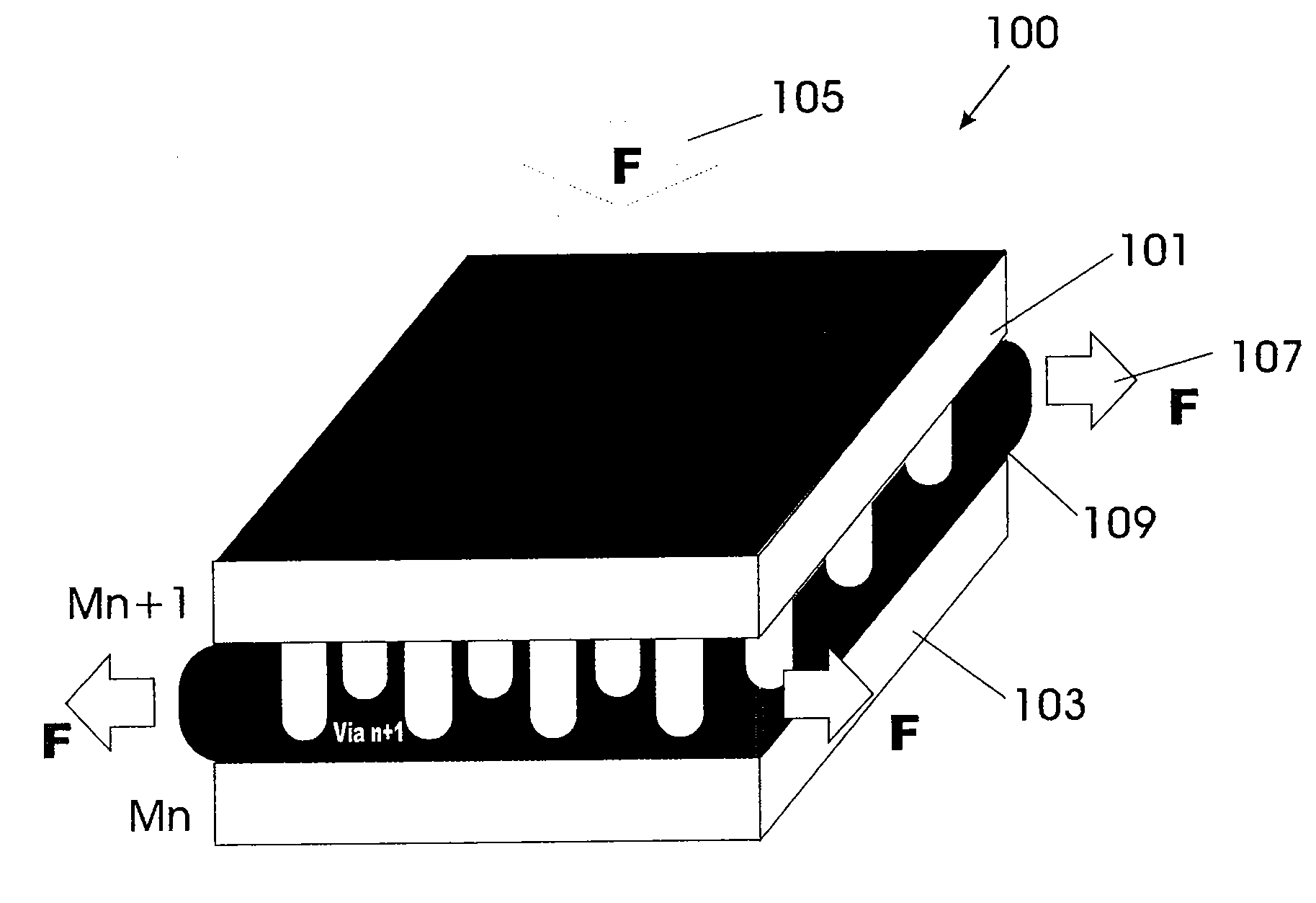
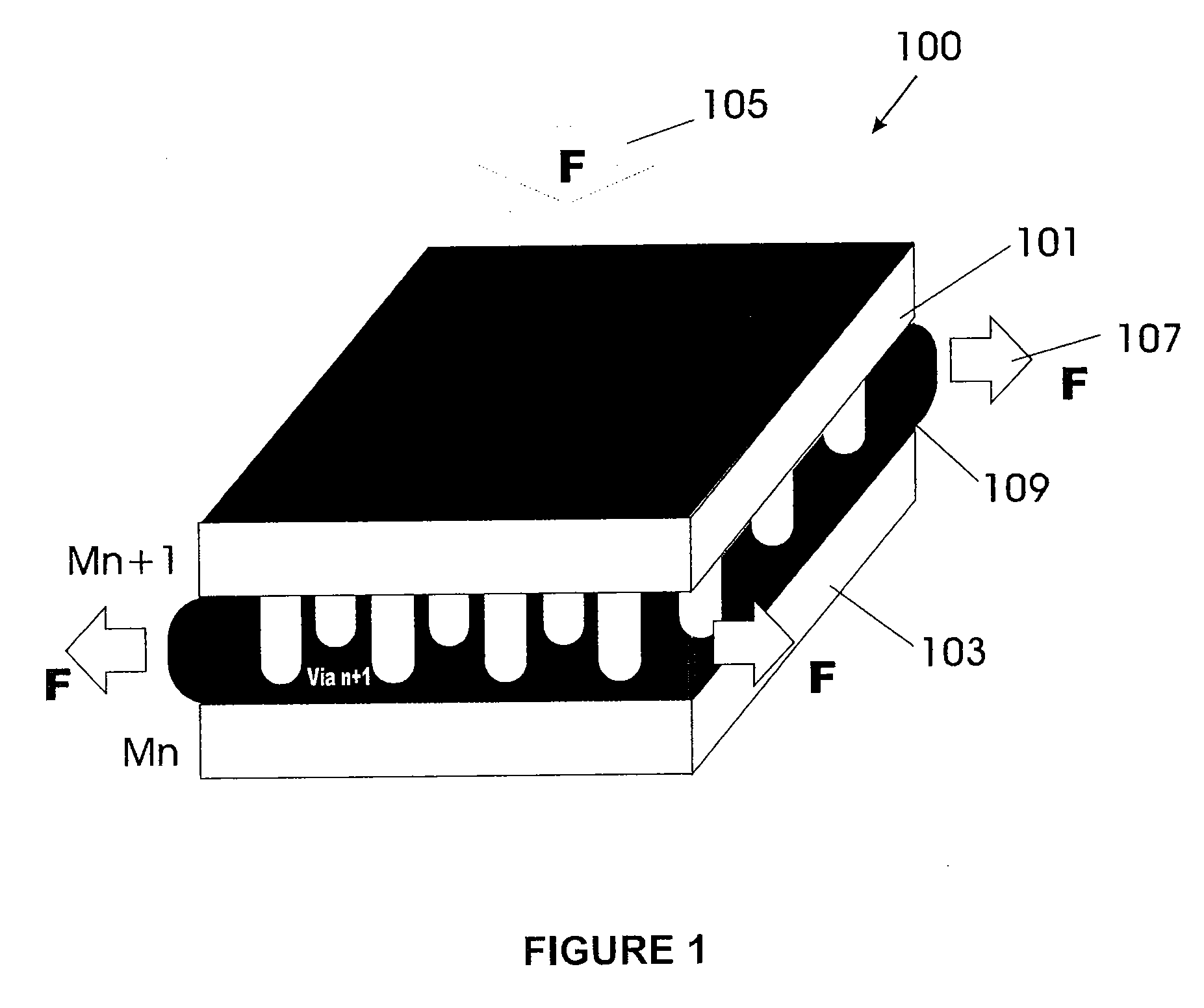
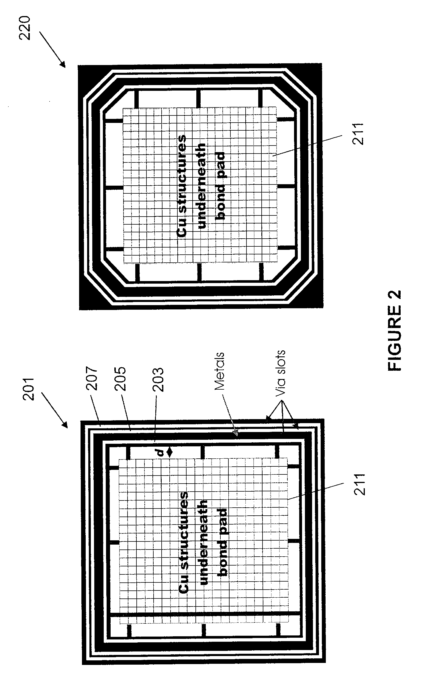
[0030]According to the present invention, techniques directed to integrated circuits and their processing for the manufacture of semiconductor devices are provided. In particular, the invention provides a method and structures for manufacturing metal interconnect structures for integrated circuit devices. More particularly, the invention provides one or more dummy structures to maintain a dielectric layer within a predefined region and between a pair of metal layers according to a specific embodiment. But it would be recognized that the invention has a much broader range of applicability.

[0031]Copper wires are usually embedded in the dielectric materials by damascene technologies, such as dual damascene structures. Since circuit structures including the embedded copper and dielectric materials often have a large difference in thermal expansion coefficients and modulus, such structures often suffer from deformation during thermal cycles during wafer processes and during the final pac...


PUM


Abstract

A method for fabricating a semiconductor device. The method includes providing a semiconductor substrate including a surface region. The method forms a first interlayer dielectric overlying the surface region and forms an interconnect layer overlying the first interlayer dielectric layer. The method also forms a low K dielectric layer overlying the interconnect layer, which has a predetermined shape. The method forms a copper interconnect layer overlying the low K dielectric layer. In a preferred embodiment, the low K dielectric layer maintains the predetermined shape using a dummy pattern structure provided within a portion of the low K dielectric layer to mechanically support and maintain the predetermined shape of the low K dielectric layer between the interconnect layer and the copper interconnect layer.

Description

CROSS-REFERENCES TO RELATED APPLICATIONS[0001]This patent application claims priority to Chinese Patent Application Number 200510111998.3; filed on Dec. 22, 2005, commonly assigned, and hereby incorporated by reference for all purposes.STATEMENT AS TO RIGHTS TO INVENTIONS MADE UNDER FEDERALLY SPONSORED RESEARCH OR DEVELOPMENT[0002]NOT APPLICABLEREFERENCE TO A “SEQUENCE LISTING,” A TABLE, OR A COMPUTER PROGRAM LISTING APPENDIX SUBMITTED ON A COMPACT DISK.[0003]NOT APPLICABLEBACKGROUND OF THE INVENTION[0004]The present invention is directed to integrated circuits and their processing for the manufacture of semiconductor devices. In particular, the invention provides a method and structures for manufacturing metal interconnect structures for integrated circuit devices. More particularly, the invention provides one or more dummy structures to maintain a dielectric layer within a predefined region and between a pair of metal layers according to a specific embodiment. But it would be reco...

Claims


Application Information

Patent Timeline
IPC IPC(8): H01L23/52H01L21/4763
CPCH01L21/76801H01L2224/05556H01L23/53228H01L24/03H01L24/05H01L2224/05093H01L2224/05096H01L2224/05624H01L2924/01005H01L2924/01013H01L2924/01014H01L2924/01025H01L2924/01029H01L2924/01033H01L2924/01075H01L2924/01082H01L2924/14H01L23/522H01L2924/10253H01L2924/01023H01L2924/01019H01L2924/01006H01L2924/00014H01L2924/00
Inventor NING, XIAN J.
Owner SEMICON MFG INT (SHANGHAI) CORP
Why Eureka
Try Eureka