
Semiconductor integrated circuit

Inactive Publication Date: 2008-06-19
ELPIDA MEMORY INC
View PDF6 Cites 8 Cited by
  • Summary
  • Abstract
  • Description
  • Claims
  • Application Information

AI Technical Summary

Benefits of technology

[0022]In FIG. 10, a capacitance element region 13 is provided in an internal element region 12 and, further, a terminal capacitance region 14 is provided in a pad region 10, thereby forming a terminal capacitance. The terminal capacitance is formed along sides of the pad region 10 except its side adjacent to a leading region 11. If the capacitance can be further added in the terminal capacitance region 14 of the pad region 10, it is possible to reduce the capacitance element region 13 of the internal element region 12. This makes it possible to effectively use the internal element region 12 and, thus, a reduction in chip size can be achieved.
[0024]Among them, it is considered best to form the capacitance using the aluminum interconnection. In the case of the capacitance using the aluminum interconnection, the antenna standard for preventing charge-up breakdown and the ESD withstand voltage standard for preventing electrostatic breakdown can be easily satisfied and thus the reliability is high. Further, it can be pointed out that the capacitance dependence of voltage and the process variation are small. However, in order to provide the capacitance using the aluminum interconnection in the terminal capacitance region 14 of the pad region 10, a design should be made so as to provide a sufficient distance from the aluminum interconnection for preventing the foregoing aluminum pattern short circuit. As a result, there is also a drawback that the capacitance possessed by the aluminum interconnection itself and the side-wall capacitance with the counter-electrode aluminum pattern are small.
[0026]Currently, the distances D2 and D3 are set large because of the pad peripheral region. By reducing these distances, an increase in capacitance value is expected. By increasing the terminal capacitance formed at the pad portion, it becomes possible to reduce the capacitance element region 13 of the internal element region 12 described with reference to FIG. 10. By reducing the capacitance element region 13, the chip size reduction is achieved. It becomes possible to reduce the distance between the bonding pad and the pad peripheral interconnection and further to form the terminal capacitance in the pad region.
[0027]It is an object of this invention to provide a bonding pad and a semiconductor integrated circuit that can reduce the distance between the bonding pad and a pad peripheral interconnection to thereby reduce the chip size. Further, it is another object of this invention to provide a bonding pad and a semiconductor integrated circuit that can reduce the distance between interconnections in a region around the bonding pad, i.e. the bonding pad peripheral region, to form a terminal capacitance, thereby reducing the chip size.

Problems solved by technology

Accordingly, as shown in FIG. 8B, there arises a problem that the aluminum pattern is offset to cause a short circuit with the pad peripheral aluminum interconnection 9.
This problem causes disadvantages such as a reduction in assembly yield and occurrence of market claims.
Consequently, the size reduction of the bonding pad peripheral region cannot be achieved.

Method used


Image

  • Semiconductor integrated circuit
  • Semiconductor integrated circuit
  • Semiconductor integrated circuit

Examples


first exemplary embodiments

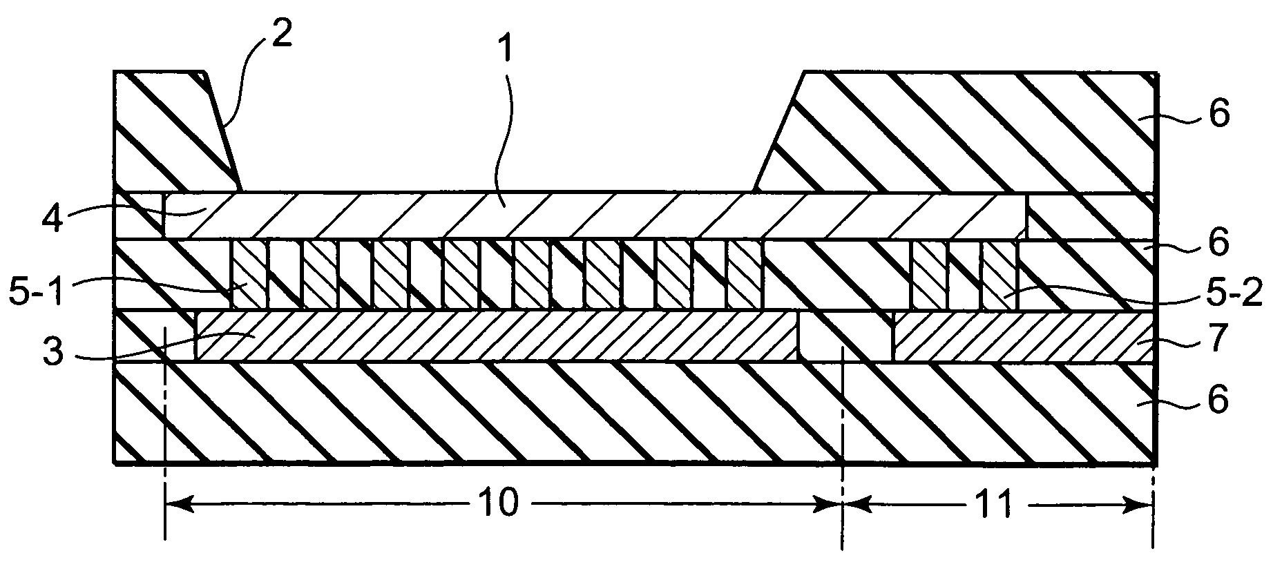
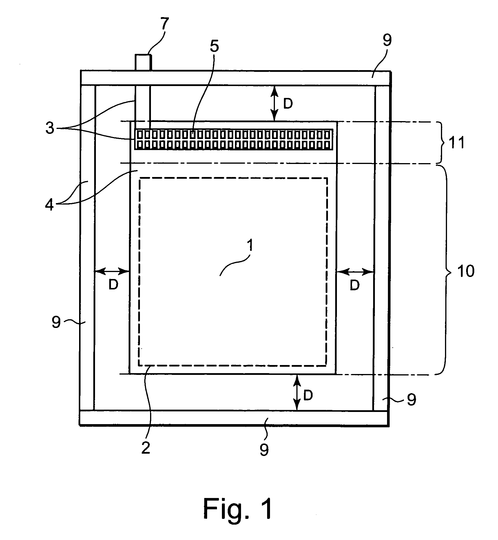
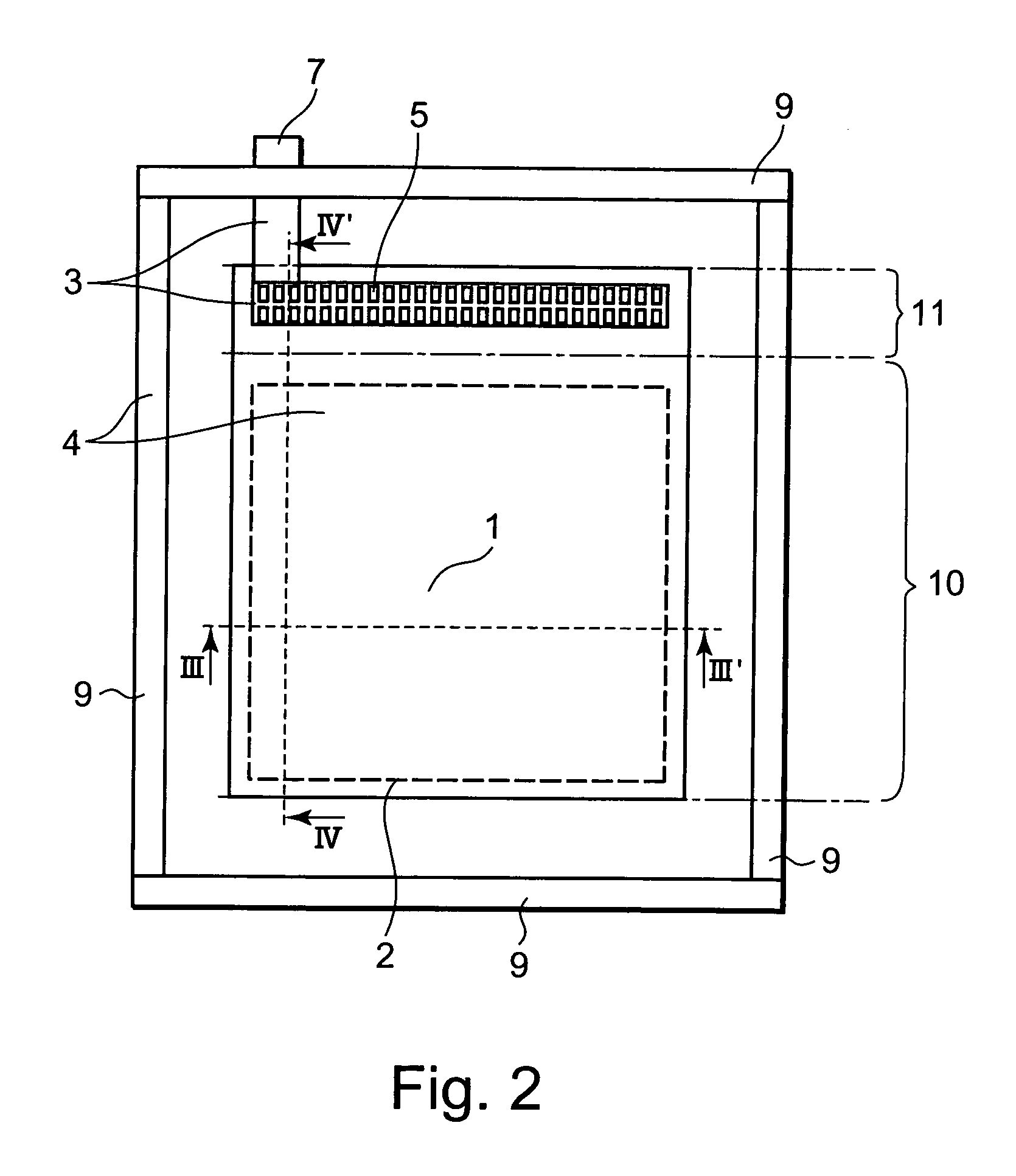
[0065]The first exemplary embodiments of this invention will be described in detail with reference to FIGS. 12 to 19D. In each embodiment, a conductive pattern / patterns is / are disposed between a bonding pad and an internal circuit connecting interconnection, and the conductive pattern / patterns and the bonding pad are connected to each other through leading interconnections. FIG. 12 is a plan view of a bonding pad portion in which leading interconnections are provided at two positions between a bonding pad and conductive patterns. FIG. 13A is a plan view for explaining an impact on bonding at the related bonding pad portion and FIG. 13B is a perspective view showing a section taken along line B-B′ in FIG. 13A. FIG. 14A is a plan view for explaining an impact on bonding at a bonding pad portion of this invention, FIG. 14B is a perspective view showing a section taken along line B-B′ in FIG. 14A, and FIG. 14C is a sectional view taken along line C-C′ in FIG. 14A. FIGS. 15A, 16A, . . . ...

second exemplary embodiments

[0078]The second exemplary embodiments of this invention will be described in detail with reference to FIGS. 20 to 28D. In each embodiment, conductive patterns are applied to capacitance pad interconnections of a terminal capacitance provided in a bonding pad region. FIG. 20 is a plan view of a bonding pad portion in which pillar-shaped leading interconnections connected to conductive patterns, respectively, are provided at two positions along each of three sides of a bonding pad. FIG. 21A is a plan view of a bonding pad portion in which pillar-shaped leading interconnections are provided at three positions along each of three sides of a bonding pad, and FIGS. 21B and 21C are sectional views taken along line B-B′ and line C-C′ in FIG. 21A, respectively. FIGS. 22A, 23A, . . . , and 28A are plan views of various bonding pad portions in each of which pillar-shaped leading interconnections are provided at positions along each of three sides of a bonding pad. FIGS. 22B, 23B, . . . , and ...


PUM


Abstract

A conductive pattern is provided in the vicinity of a bonding pad and connection is made therebetween using pillar-shaped leading interconnections. By providing an insulating film, in addition to the pillar-shaped leading interconnections, between the conductive pattern and the bonding pad, the impact at the time of bonding is weakened to thereby suppress offset of the conductive pattern. According to the pad structure of this invention, it becomes possible to reduce the pattern design standard around the bonding pad and thus a small-chip-size semiconductor integrated circuit is obtained.

Description

[0001]This application is based upon and claims the benefit of priority from Japanese patent application No. 2006-340791, filed on Dec. 19, 2006, the disclosure of which is incorporated herein in its entirety by reference.BACKGROUND OF THE INVENTION [0002]This invention relates to a semiconductor integrated circuit and, in particular, relates to the layout and structure of a bonding pad and its peripheral interconnection.[0003]A semiconductor integrated circuit has a plurality of connection terminals (leads) for data transfer with an external system. By connecting these connection terminals to bonding pads provided on a semiconductor substrate by wire bonding, an internal circuit of the semiconductor integrated circuit and the external system are connected together. Since, in this wire bonding, a wire is mechanically bonded to the bonding pad under pressure, the bonding pad is required to have a large size. Further, the pad peripheral standard that is much more lenient than the norm...

Claims


Application Information

Patent Timeline
IPC IPC(8): H01L23/488
CPCH01L23/5223H01L2224/05553H01L24/05H01L27/0248H01L2224/05001H01L2224/05093H01L2224/05095H01L2224/05096H01L2224/05624H01L2924/01004H01L2924/01005H01L2924/01013H01L2924/01082H01L2924/14H01L2924/30105H01L24/03H01L2224/02166H01L2924/01033H01L2924/01006H01L2924/00014
Inventor YASUMORI, KOJINAGAMINE, HISAYUKI
Owner ELPIDA MEMORY INC
Features
  • Generate Ideas
  • Intellectual Property
  • Life Sciences
  • Materials
  • Tech Scout
  • Unparalleled Data Quality
  • Higher Quality Content
  • 60% Fewer Hallucinations
Learn More