Pixel Clock Generator, Pulse Modulator, and Image Forming Apparatus

a pulse modulator and clock generator technology, applied in the direction of instruments, electrographic processes, optical elements, etc., can solve the problems of image quality degradation, color reproduction and resolution degradation, and error due to variation in average scanning

Inactive Publication Date: 2008-06-19
RICOH KK
View PDF4 Cites 26 Cited by
  • Summary
  • Abstract
  • Description
  • Claims
  • Application Information

AI Technical Summary

Benefits of technology

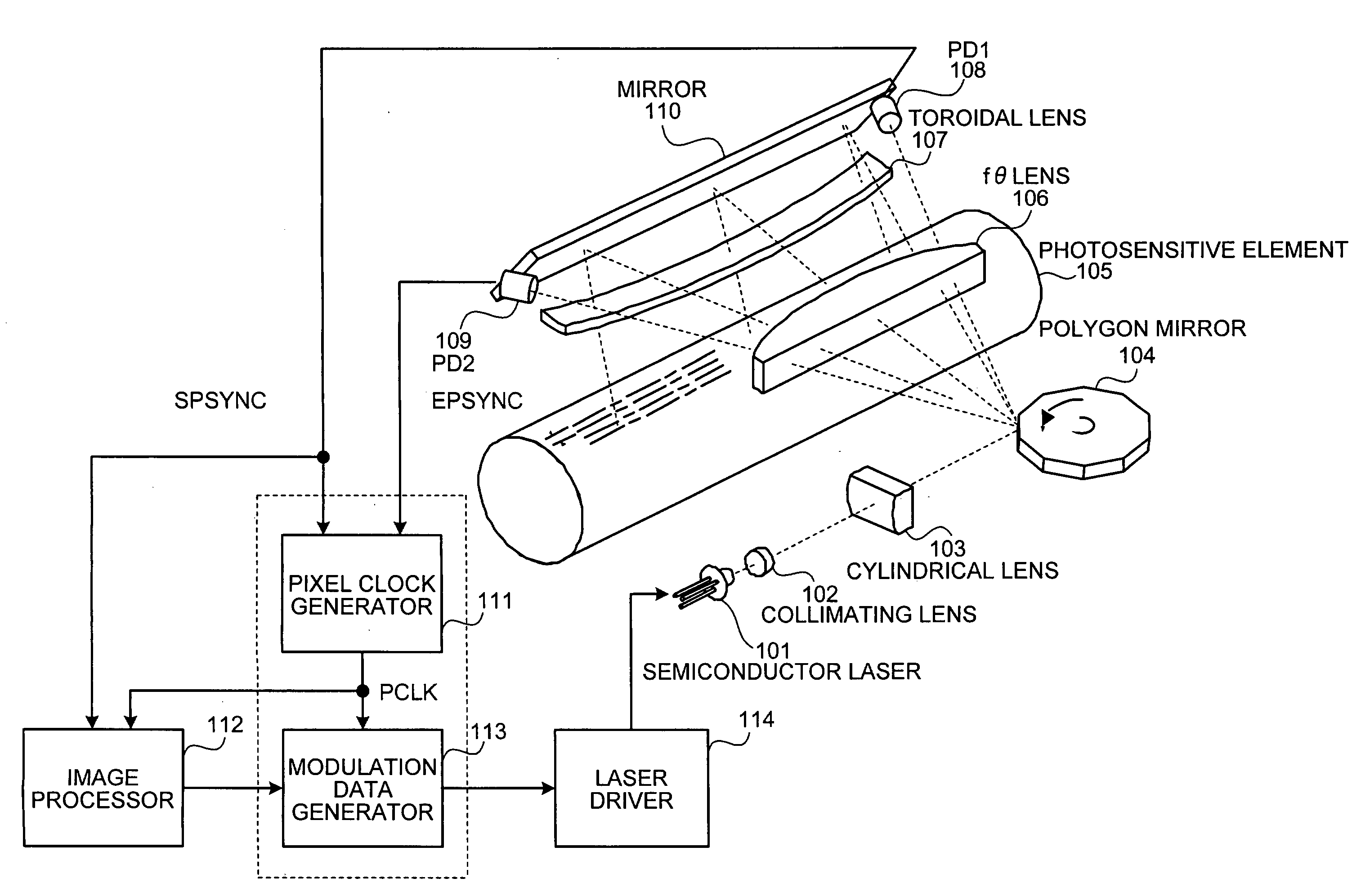
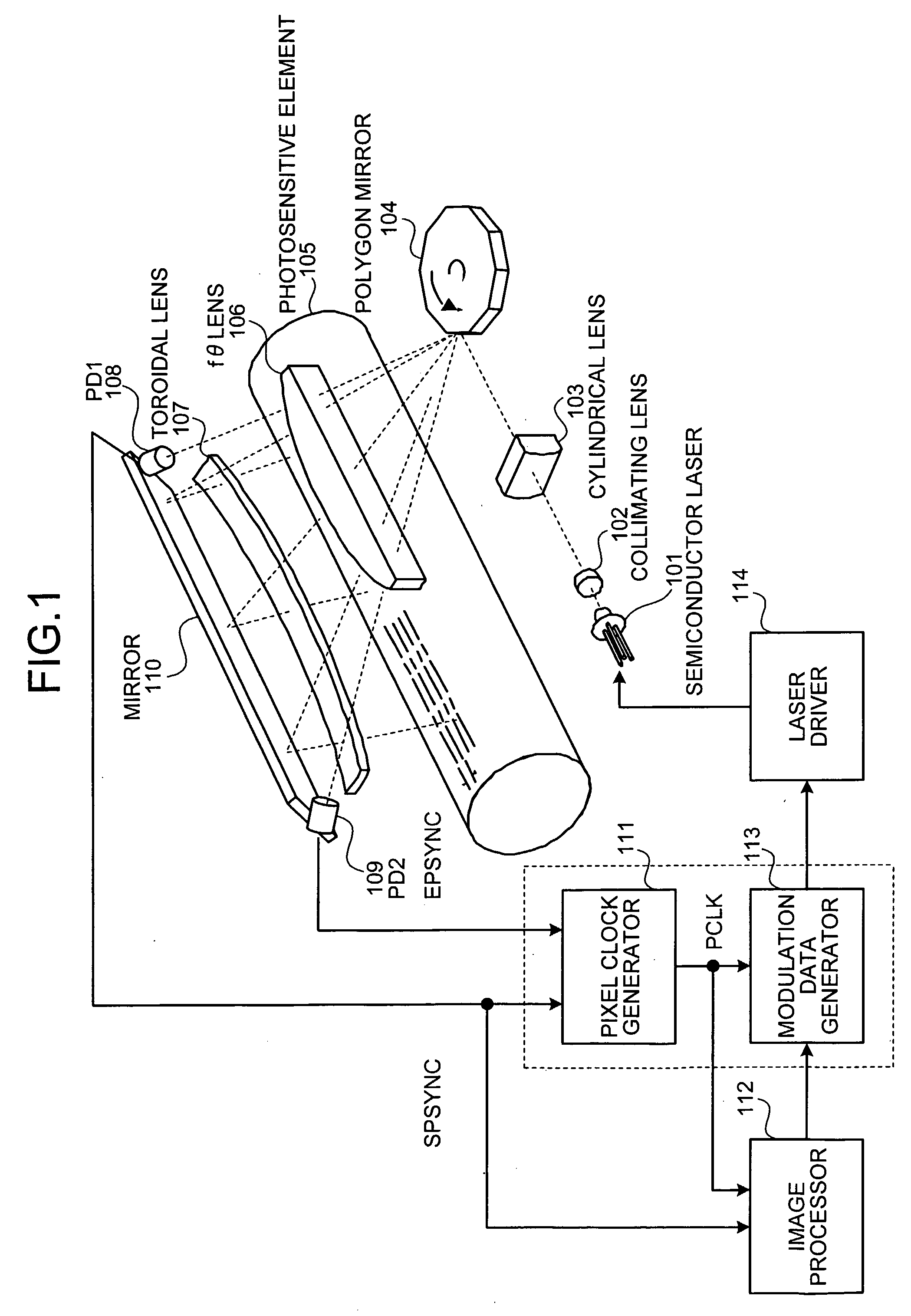
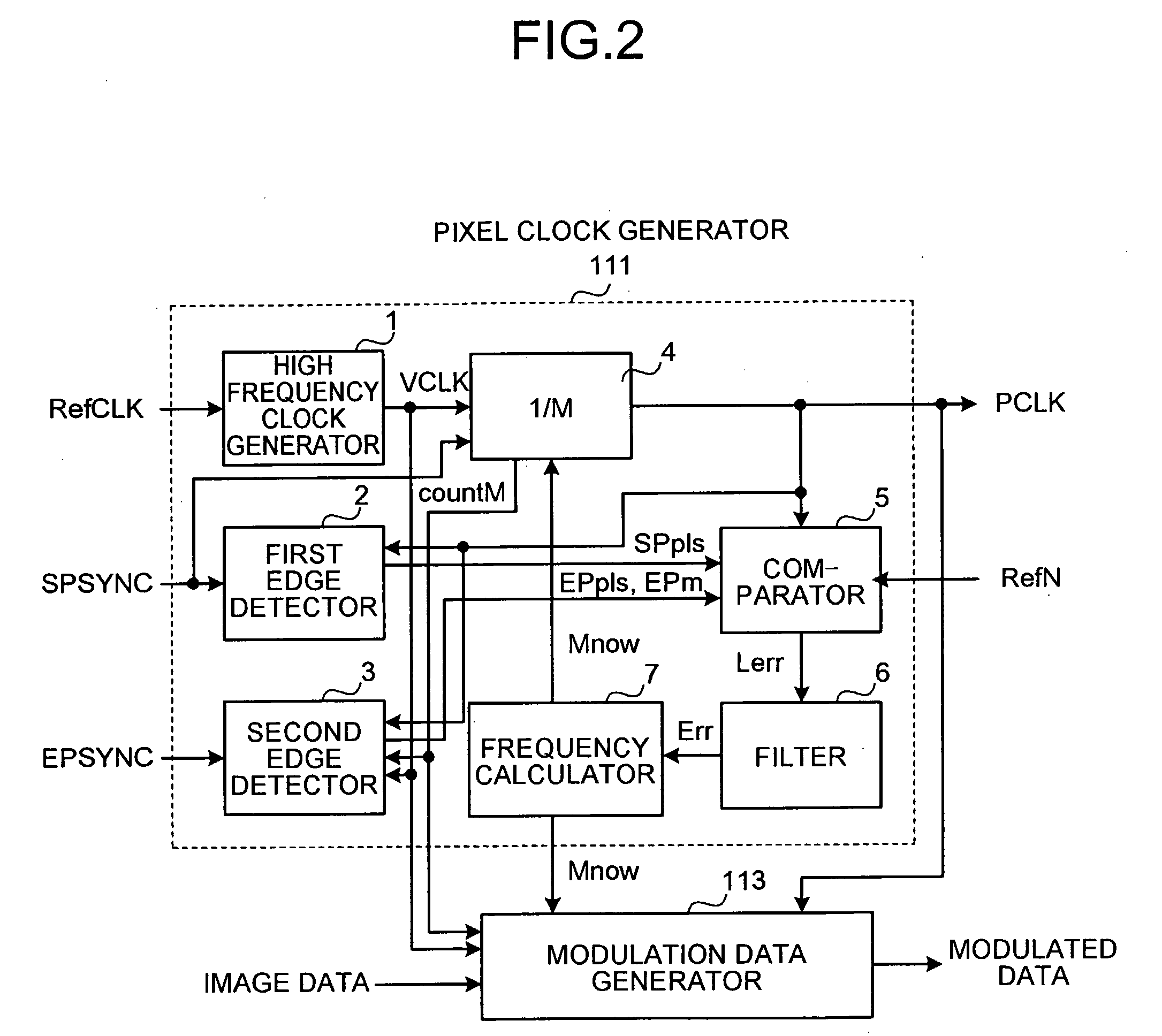
[0025]According to an embodiment of the present invention, a pixel clock is generated based on a high frequency clock, and a pixel clock frequency is controlled according to a variation in scanning time. Therefore, it is possible to generate a pixel clock allowing correction of an error due to the variation with high accuracy even if average scanning speed varies.

Problems solved by technology

In such a scanning optical system, variations of scanning speed cause fluctuations in an image, which leads to degradation of image quality.
Particularly, in a color image, a dot offset of each color occurs in a main scanning direction, which leads to color shift, and the color shift causes degradation of color reproduction and degradation of resolution.
This type of error is an error with a periodicity of several lines, for example, the number of lines for the number of facets of a polygon mirror.
(2) Error Due to Variations in Average Scanning Speed
This type of error includes scanning speed variations which occur in a multi-beam optical system that has a plurality of light sources such as a semiconductor laser array and that concurrently scans a plurality of light beams by a common scanning optical system.
(4) Error of Each Scanning Optical System
The main factor of this type includes deformation due to low manufacturing accuracy and assembly accuracy of the parts for the scanning optical systems and also due to change in the parts with time.
Furthermore, because the light sources are different from each other, the error (3) may occur.
This error is such that the average scanning speeds are different from each other and further the errors (1) and (2) discretely occur.
Although some of image forming apparatuses include those in which part of units in the scanning optical system is shared, light paths from respective light sources to each medium to be scanned (photosensitive element) are different from each other, and hence, this error is also included in this error (4).
There have been some problems as follows about conventional control technology for pixel clock frequency.
Therefore, it is not possible to ensure a sufficient open loop gain of PLL (Phase Locked Loop) and to obtain satisfactory control accuracy.
Furthermore, this frequency is weak in disturbance and the clock frequency thereby fluctuates, and therefore, a clock with high precision cannot be generated.

Method used


Image

  • Pixel Clock Generator, Pulse Modulator, and Image Forming Apparatus
  • Pixel Clock Generator, Pulse Modulator, and Image Forming Apparatus
  • Pixel Clock Generator, Pulse Modulator, and Image Forming Apparatus

Examples


fourth embodiment

[0222]An image forming apparatus according to a fourth embodiment of the present invention has a different point from the first embodiment in that the image forming apparatus includes a plurality of photosensitive elements for multiple color. The image forming apparatus has photosensitive elements separately provided corresponding to colors of cyan, magenta, yellow, and black, has a plurality of scanning optical systems provided corresponding to the respective photosensitive elements, and forms images (electrostatic latent images) corresponding to the colors on the photosensitive elements respectively. The images of the colors are transferred to one image forming medium (e.g., paper) to form a color image.

[0223]FIG. 24 is a schematic diagram of mainly a mechanical operation portion of the image forming apparatus according to the fourth embodiment. FIG. 25 is a schematic diagram of mainly an image processing portion of the image forming apparatus according to the fourth embodiment.

[0...


PUM


Abstract

A comparator compares a time interval between a first synchronization signal and a second synchronization signal with a target value, and outputs an error therebetween. A frequency calculator calculates a set value of a pixel clock frequency based on the error output from the comparator, and outputs a frequency specification signal for specifying a pixel clock frequency according to the calculated set value. A frequency divider divides a high frequency clock generated by a high frequency clock generator by a frequency division ratio based on the frequency specification signal output from the frequency calculator, and generates the pixel clock.

Description

TECHNICAL FIELD[0001]The present invention relates to a pixel clock generator, a pulse modulator, and an image forming apparatus.BACKGROUND ART[0002]FIG. 28 is a general schematic diagram of a conventional image forming apparatus. The image forming apparatus shown in FIG. 28 is a laser printer or a digital copier. A laser beam emitted from a semiconductor laser unit 1009 is scanned by a rotating polygon mirror 1003, to form a beam spot on a photosensitive element 1001 which is a medium to be scanned through a scanning lens 1002, and exposes the photosensitive element 1001 to form an electrostatic latent image thereon. At this time, a photodetector 1004 detects a scanning beam in each line.[0003]A phase synchronization circuit 1006 receives a clock from a clock generation circuit 1005, generates an image clock (pixel clock) of which phase is synchronized in each line, and supplies the image clock to an image processing unit 1007 and a laser drive circuit 1008. The semiconductor laser...

Claims


Application Information

Patent Timeline
Patent Type & Authority Applications(United States)
IPC IPC(8): B41J2/435
CPCG02B26/127G06K15/1219H04N1/0473H04N2201/0082H04N2201/04791H04N2201/04794H04N2201/04755G03G15/04G02B26/10
Inventor MASUI, NARUHIROEMA, HIDETOSHITSUKAMOTO, NOBUNARI
Owner RICOH KK
Why Eureka
Try Eureka