Vertical cavity surface emitting semiconductor laser device

a laser device and vertical cavity technology, applied in semiconductor lasers, laser details, electrical equipment, etc., can solve the problems of small refractive index difference between a pair of semiconductors of the dbr layer made of semiconductors and long wavelength vertical cavity surface emitting lasers

Active Publication Date: 2008-06-19
LUMENTUM JAPAN INC
View PDF3 Cites 10 Cited by
  • Summary
  • Abstract
  • Description
  • Claims
  • Application Information

AI Technical Summary

Benefits of technology

[0018]FIG. 6 is a structural view showing an example of the present invention.
[0019]FIG. 7 is a structural view showing an example of the present invention.
[0020]FIG. 8 is a structural view showing an example of the present invention.
[0021]101: n-type InP substrate, 102: n-type semiconductor DBR (distributed Bragg-reflector) layer(s), 102a: n-type InP layer, 102b: InGaAlAs-MQW (multi-quantum-wells) layer, 103: n-type spacer layer, 104: MQW active layer, 105: p-type spacer layer, 106: p-type InP layer, 107: n-type InP layer, 108: n-type InGaAs contact layer, 109: SiO2 passivation layer, 110: dielectric DBR layer (s), 111: InGaAlAs-tunnel junction, 111a: n+-type InGaAlAs layer, 111b: p+-type InGaAlAs layer, 112: electrode for n-type semiconductor, 113: electrode for n-type semiconductor, 201: InGaAlAs-well, 202: InGaAlAs-barrier, 301: n-type GaAs substrate, 302: n-type DBR layer (s), 302a: n-type Al0.9Ga0.1As layer, 302b: n-type Al0.15Ga0.85As layer, 303: n-type Al0.3Ga0.7As-spacer layer, 304: GaAs / Al0.3Ga0.7As MQW, 305: p-type Al0.3Ga0.7As-spacer layer, 306: AlOx-oxidation layer, 307: p-type DBR layer(s), 307a: p-type Al0.9Ga0.1As layer, 307b: p-type Al0.15Ga0.85As layer, 308: p+-type GaAs layer, 309: SiO2 passivation layer, 310: electrode for p-type semiconductor, 311: electrode for n-type semiconductor, 601: bulk DBR layer(s), 601a: n-type InP layer, 601b: n-type InGaAlAs layer, 701: undoped bulk DBR layer(s), 701a: undoped InP layer, 701b: undoped InGaAlAs layer, 801: DBR layer(s), 801a: undoped InP layer, 801b: air gap layer

Problems solved by technology

On the other hand, many of the long wavelength vertical cavity surface emitting lasers in the range from 1.3 μm band to 1.55 μm band applicable to optical fiber communications are still in the research stage and have not become popular.
One of the reasons why the long wavelength vertical cavity surface emitting lasers are still in the research stage is due to a problem that in the long wavelength vertical cavity surface emitting lasers the refractive index difference in a pair of semiconductors of the DBR layer made of semiconductor is small.
However, as the wavelength that defines a composition of a compound semiconductor is increased, the light absorption of the layer increases due to the oscillation wavelength of the laser, resulting in a problem that the effective reflectivity cannot be increased.
Particularly, this problem becomes significant in the case where the DBR layer is doped with impurities so that the current can be injected into the active layer through the DBR layer(s).

Method used


Image

  • Vertical cavity surface emitting semiconductor laser device
  • Vertical cavity surface emitting semiconductor laser device
  • Vertical cavity surface emitting semiconductor laser device

Examples


example 1

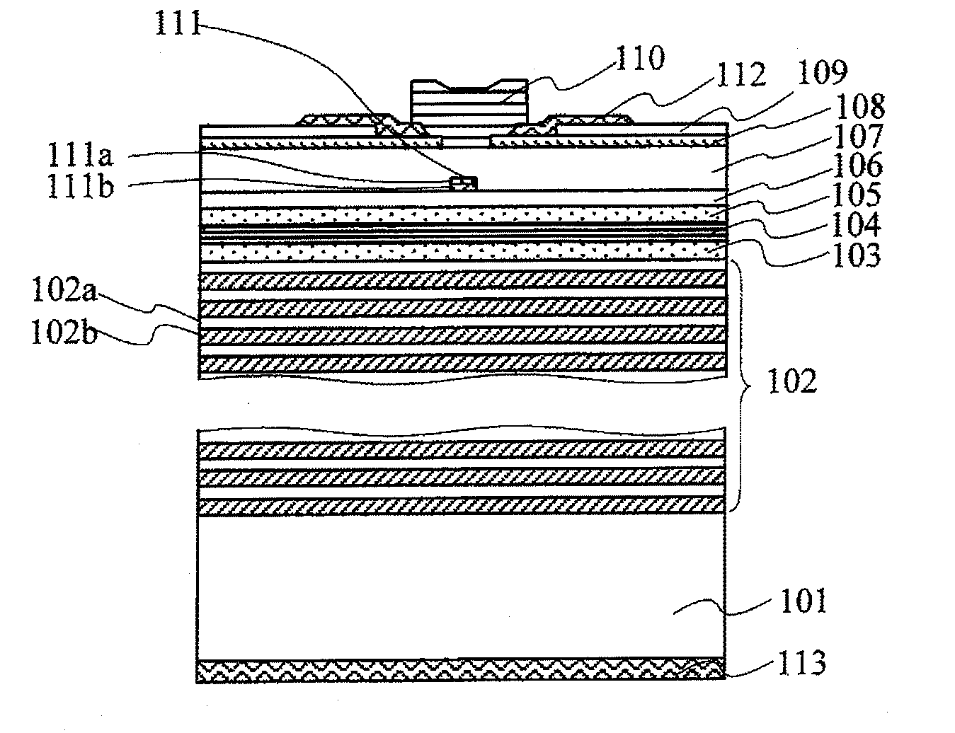
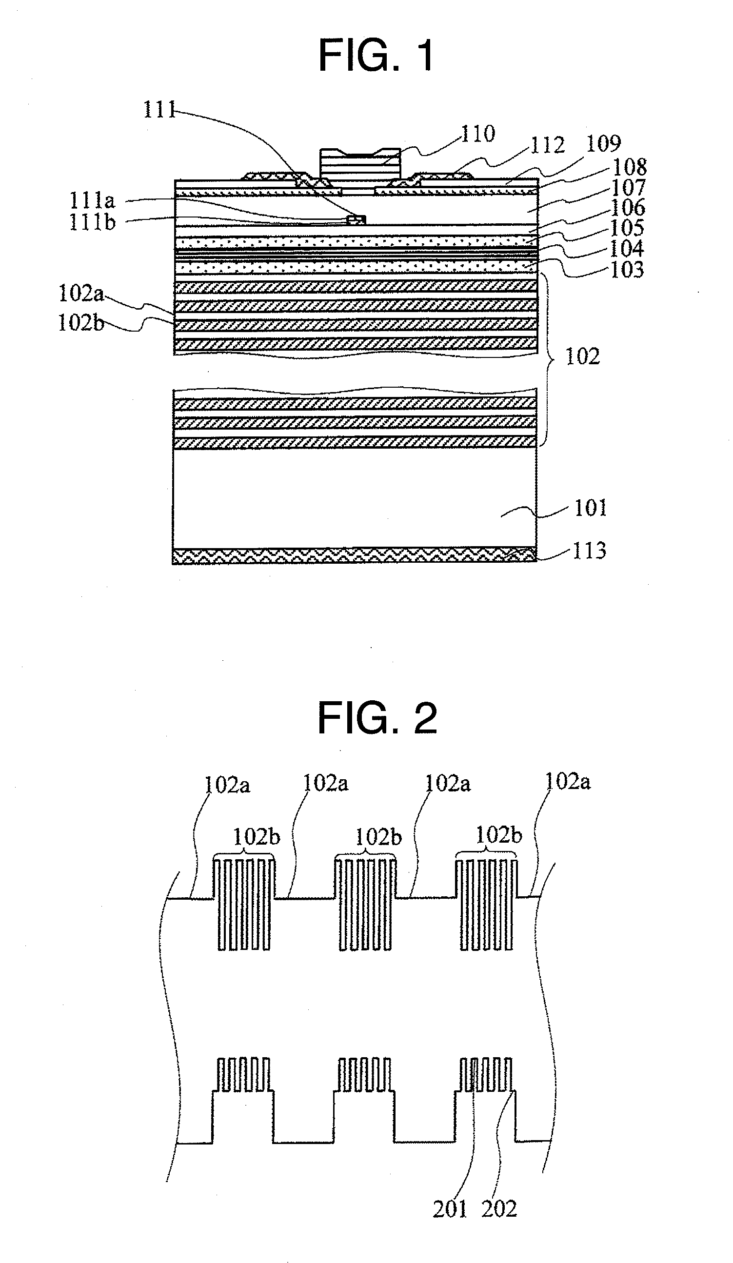
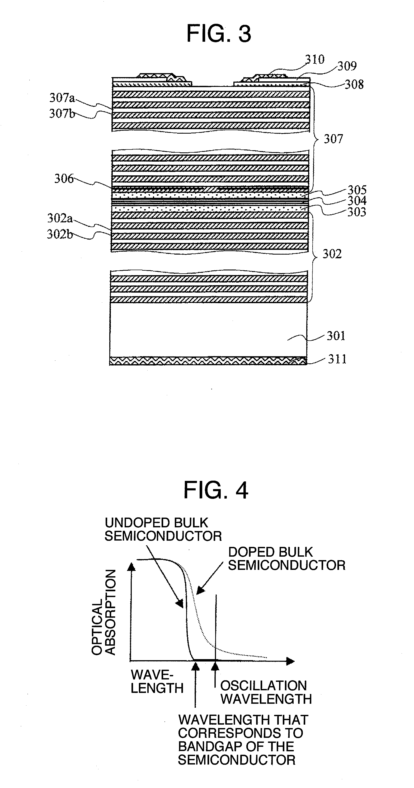
[0030]Example 1 is an example in the case where the present invention is applied to a vertical cavity surface emitting laser of 1.3 μm band for optical fiber communications. FIG. 1 is a schematic view of this cross-sectional structure. In FIG. 1, an n-type semiconductor DBR layer(s) 102 is laminated on an n-type InP substrate 101. The DBR layer(s) 102 is composed of a pair of semiconductor layers of an InP layer 102a and an InGaAlAs multi-quantum-wells layer 102b, and the number of pairs thereof is set to 45, and the reflectivity is 99.5%. On the DBR layer(s) 102, an n-type spacer layer 103, an InGaAlAs quantum well active layer 104, and a p-type spacer layer 105 are laminated in the order. Moreover, on top thereof is laminated a p-type InP layer 106. In part on the p-type Inp layer 106 is formed a tunnel junction 111 having the wavelength that defines a composition of a compound semiconductor of 1.15 μm. The tunnel junction is a pn junction in which high-concentration n-type impuri...

example 2

[0038]Example 2 is an example in the case where the present invention is applied to a vertical cavity surface emitting laser of 1.3 μm band for optical fiber communications. FIG. 6 is a schematic view of this cross-sectional structure. The structure above the DBR layer(s) 102 is the same as that of Example 1. However, in this example, the number of semiconductor layer pairs of the n-type InP layer 102a and n-type InGaAlAs multi-quantum-wells layer 102b in the DBR layer(s) 102 is 10 pairs, and a bulk DBR layer(s) 601 is formed below the DBR layer(s) 102. The bulk DBR layer(s) 601 has a structure in which 35 pairs of n-type InP layer 601a and n-type InGaAlAs layer 601b are laminated alternatively, the n-type InGaAlAs layer 601b being a bulk and of which the wavelength that defines a composition of a compound semiconductor being 1.18 μm. The lamination of the DBR layer(s) 102 and bulk DBR layer(s) 601 can provide a reflectivity of 99.5%. It takes skills and time to manufacture the InGa...

example 3

[0039]Example 3 is an example in the case where the present invention is applied to a vertical cavity surface emitting laser of 1.3 μm band for optical fiber communications. FIG. 7 is a schematic view of this cross-sectional structure. The structure above the DBR layer(s) 102 is the same as Example(s) 1 and 2. However, as in the case of Example 2, the number of semiconductor layer pairs of the n-type InP layer 102a and n-type InGaAlAs multi-quantum-wells layer 102b in the DBR layer(s) 102 is 10 pairs in this example. An undoped bulk DBR layer(s) 701 is provided below the DBR layer(s) 102. The bulk DBR layer(s) 701 has a structure in which 35 pairs of undoped InP layer 701a and undoped InGaAlAs layer 701b are laminated alternatively, the undoped InGaAlAs layer 701b being a bulk and having the wavelength that defines a composition of a compound semiconductor of 1.18 μm. The lamination of the DBR layer(s) 102 and bulk DBR layer(s) 701 can provide a reflectivity of 99.5%. Moreover, alth...


PUM


Abstract

The relationship between the reflectivity characteristic of a DBR layer(s), in which an InP layer and an InGaAlAs layer are laminated alternatively, and the optical absorption characteristic of the InGaAlAs layer, is a trade-off in a vertical cavity surface emitting laser on an InP substrate. The present invention applies a semiconductor DBR layer(s), in which an InP layer and an InGaAlAs-MQW (multi-quantum-wells) layer are laminated alternatively, in order to dissolve the above trade-off. The InGaAlAs-MQW layer is composed of InGaAlAs-wells and barriers. The InP layer is doped uniformly and the InGaAlAs-MQW layer has a structure in which at least a part thereof is doped.

Description

INCORPORATION BY REFERENCE[0001]The present application claims priority from Japanese application JP2006-335252 filed on Dec. 13, 2006, the content of which is hereby incorporated by reference into this application.FIELD OF THE INVENTION[0002]The present invention relates to vertical cavity surface emitting semiconductor laser devices, particularly laser devices using semiconductor, more particularly semiconductor lasers for optical communication, modulators, and integrated light sources integrating the same which are used as a light source of optical fibers.BACKGROUND OF THE INVENTION[0003]The worldwide spread of the Internet is increasing the amount of the data traffic in optical communication networks year by year. To address such increase, there is a need for higher performances, such as further speed up, further reduction in power consumption and the like, in the semiconductor light sources and modulators that are key devices in optical fiber communication networks or the integ...

Claims


Application Information

Patent Timeline
Patent Type & Authority Applications(United States)
IPC IPC(8): H01S5/183
CPCB82Y20/00H01S5/06226H01S5/18308H01S5/18358H01S5/34306H01S5/305H01S5/3054H01S5/3095H01S5/18369
Inventor NAKAHARA, KOUJIADACHI, KOICHIROSHIOTA, TAKASHITSUCHIYA, TOMONOBUSHINODA, KAZUNORI
Owner LUMENTUM JAPAN INC
Why Eureka
Try Eureka