Display element and display device

a display element and display device technology, applied in the field of display elements, can solve the problems of reducing the display quality, and increasing the scale of the circuitry, and achieve the effects of suppressing the variance of luminance, suppressing the color hue, and large numerical apertur

Active Publication Date: 2008-06-26
SHARP KK
View PDF7 Cites 4 Cited by
  • Summary
  • Abstract
  • Description
  • Claims
  • Application Information

AI Technical Summary

Benefits of technology

[0011]It is thus an object of the present invention to provide a display element and a display device, with which variations in the luminance are suppressed and colored hues are suppressed while ensuring a large numerical aperture, without providing special correction circuits or conductors having a complex resistance distribution
[0020]In a display device comprising a plurality of these display elements, the balance of the current flowing from the power source line electrode through the electro-optical element can be adjusted, and the luminance variations can be kept within a predetermined tolerance range without increasing the scale of the circuitry. Therefore, a display element can be provided that has little luminance variations, a high numerical aperture, an excellent light emission efficiency, and a long lifetime.
[0023]Furthermore, it is preferable that the power source line electrode's electrode width at a portion adjacent to a region where the electro-optical element is disposed is larger than the power source line electrode's electrode width at other portions. With such a configuration, when trying to realize the above-noted resistance ratio in order to design the pixels such that they have a high numerical aperture, it is possible to set the electrode width to an extent that does not compromise the circuit configuration in regions with a relatively low degree of freedom, such as the TFT circuit portions, and to suitably adjust the electrode width in regions where the electro-optical elements are disposed, so that it becomes easy to design the pixels such that the above-noted resistance ratio condition is met.
[0037]In a display device including such display elements, a low luminance variation, a high numerical aperture, a superior light emission efficiency, and a long lifetime are achieved by adjusting a balance of the currents flowing from the power source line electrode through the electro-optical elements, without providing a separate circuit for correcting luminance variations or controlling the pixel luminance by adding a correction of the data signal. Furthermore, a uniform display without color hues can be performed.
[0039]With this configuration, the display element column can be expressed as a ladder circuit of multiple stages, and the further the display elements are from the current supply points, the lower is the applied voltage due to the electrode resistance. Thus, a large difference in luminance occurs when comparing display elements far from the current supply points and display elements near the current supply points. Therefore, by providing the power source line electrode with a plurality of current supply points, the positions of the display elements become closer to the current supply points and it is possible to further reduce the luminance variations. Furthermore, a uniform display without color hues can be performed.

Problems solved by technology

As a result, also the power consumption becomes relatively low.
Thus, since the luminance of the electro-optical element is lowered exponentially due to the above-described voltage drop, the display device suffers from conspicuous variations or irregularities in luminance, lowering the display quality.
When this correction circuit is provided in a driver portion incorporated in the display panel, the scale of the circuitry increases, which is undesirable.
When the scale of the circuitry increases, there are disadvantages with regard to the manufacturing yield, for example.
Moreover, with the configuration disclosed in JP 2001-83934A, the resistance distribution of the conductors must be set such that voltage drops due to the resistance of the conductors are suppressed, so that complex design and layout of the conductors becomes necessary.
To do so, the electrode width of the power source line should be increased in order to suppress luminance variations, but in this case, the numerical aperture is decreased, as mentioned above, worsening the light emission efficiency of the electro-optical elements.
This causes the problems that the element lifetime is shortened, and the power consumption is increased.

Method used


Image

  • Display element and display device
  • Display element and display device
  • Display element and display device

Examples


Embodiment Construction

[0058]The following is a description of preferred embodiments of the present invention, with reference to the accompanying drawings.

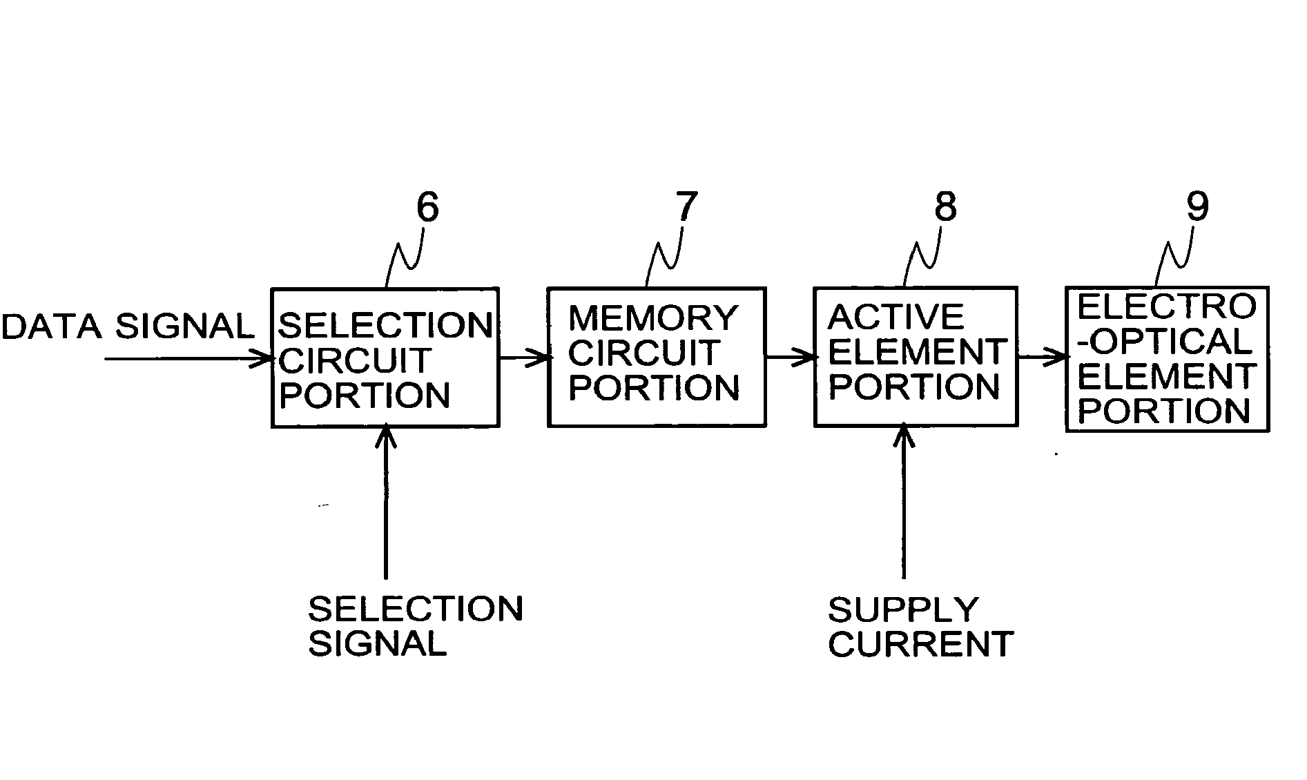
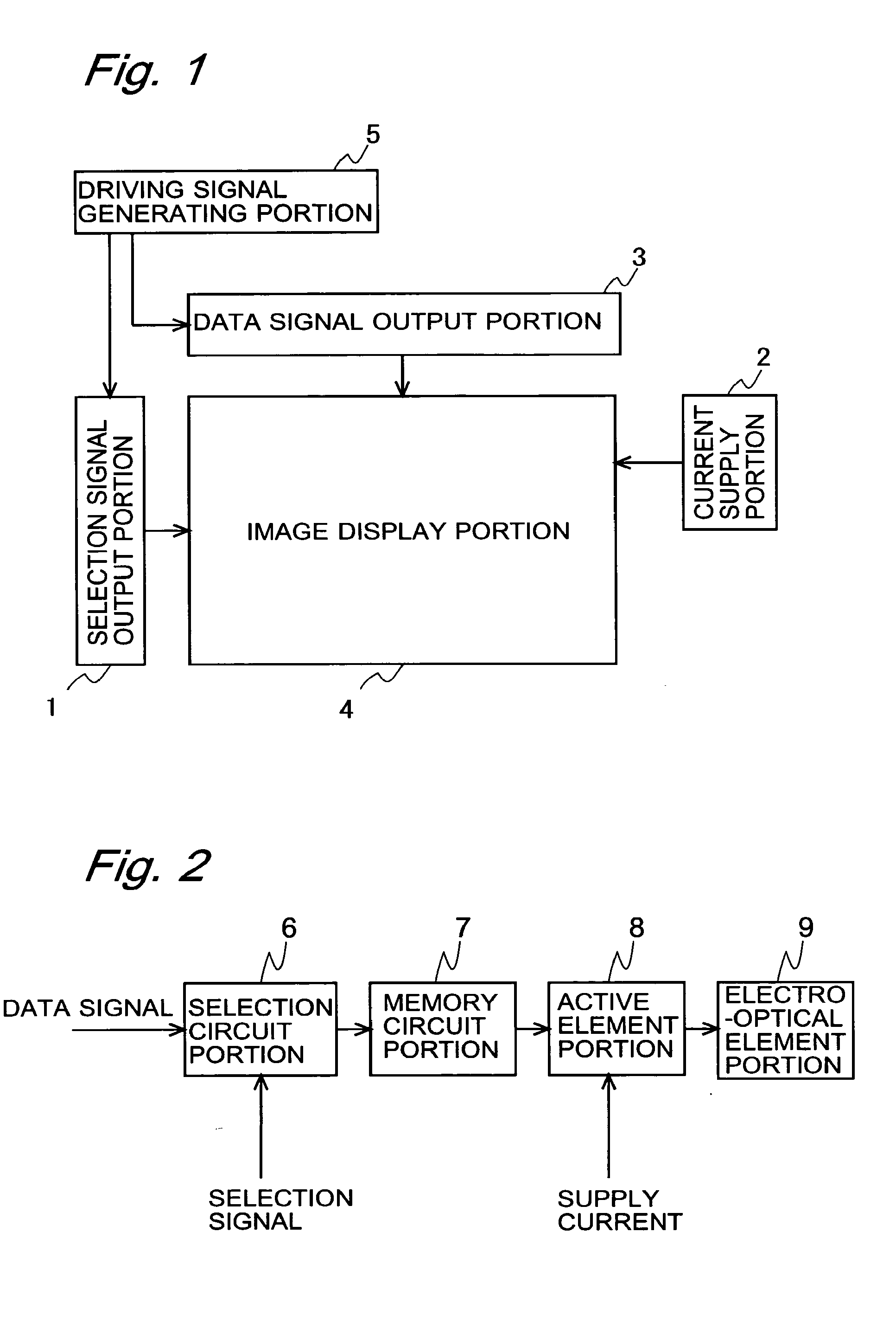
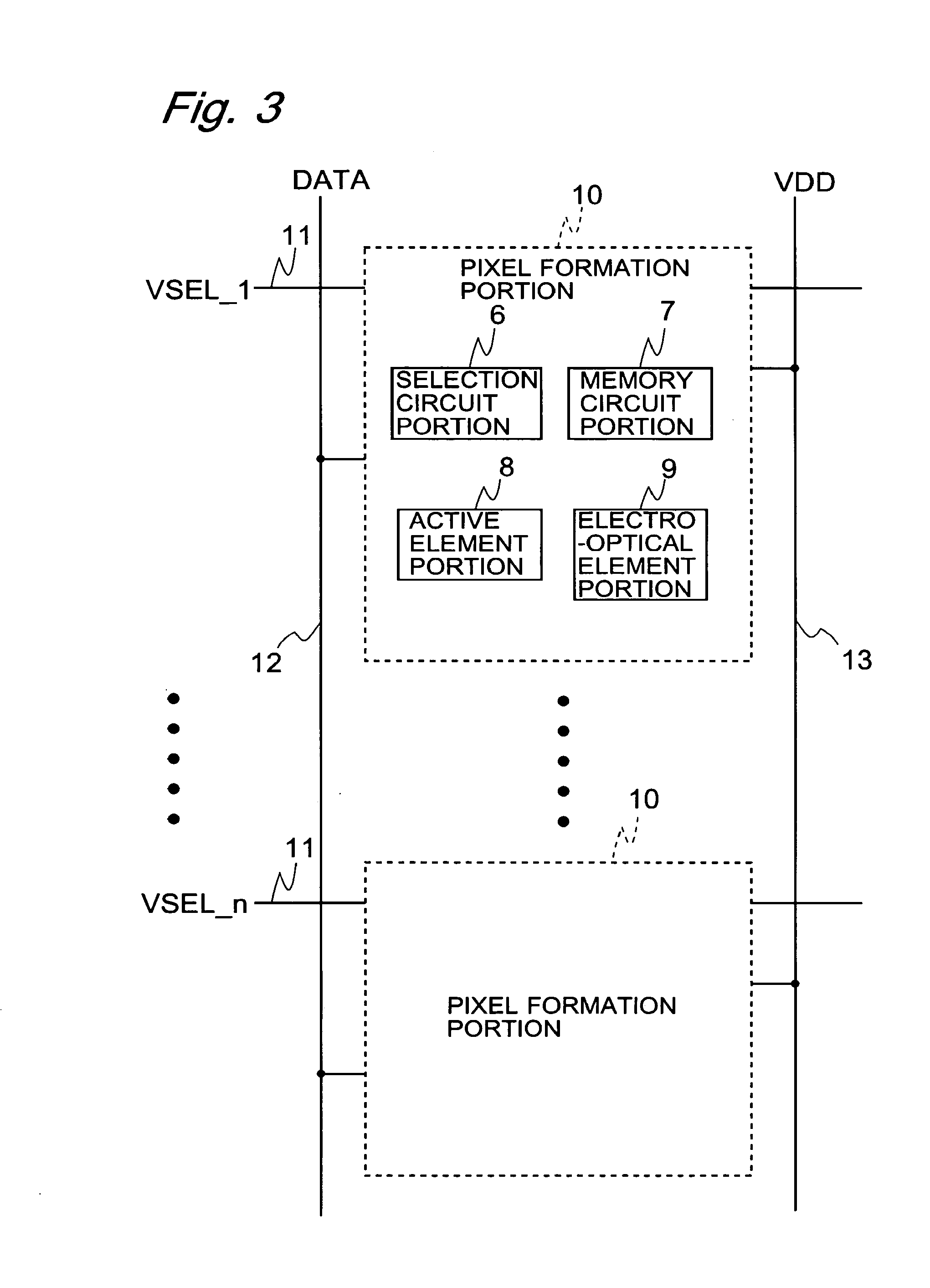
[0059]FIG. 1 is a block diagram showing the configuration of a display device according to an embodiment of the present invention. This display device includes an image display portion 1, a current supply portion 2, a data signal output portion 3, a selection signal output portion 4, and a driving signal generating portion 5. The image display portion 1 is configured by arranging a plurality of display elements, each made of a circuit including an organic EL element serving as a light emitting element, in an m×n matrix. The selection signal output portion (gate driver circuit) 4 is connected to n scanning signal lines arranged in a row direction, and outputs a scanning signal having a predetermined period to the scanning signal lines. The data signal output portion (source driver circuit) 3 is connected to m data signal lines arranged in column directio...


PUM


Abstract

A display element included in a display device is provided with a TFT circuit portion and a pixel aperture portion to which an organic EL element material is applied and which emits light in accordance with a current from the TFT circuit portion, as well as a scanning signal line electrode, a data signal line electrode and a power source line electrode. The resistance Re of the power source line electrode can be reduced, because the electrode width at a portion where the power source line electrode is in contact with the pixel aperture portion is larger than the electrode width at other portions. The resistance ratio Rx / Re between the electrode resistance Re and a combined resistance Rx of a current path from the power source line electrode through the pixel aperture portion is at least 105. Thus, a display element and a display device are realized, which have little luminance variation within the display screen, which have a high numerical aperture, a high light emission efficiency and a long lifetime.

Description

BACKGROUND OF THE INVENTION[0001]1. Field of the Invention[0002]The present invention relates to display elements in which light emission is controlled by the amount of current flowing through an electro-optical element, such as an organic EL element or an inorganic EL element, as well as to display devices including such display elements.[0003]2. Description of the Related Art[0004]To date, there are display devices whose light emission sources are electro-optical elements whose optical characteristics are changed by applying electricity, such as organic EL (electroluminescent) elements, inorganic EL elements or light emitting diodes. In such display devices, a plurality of display elements each including an electro-optical element are arranged in a matrix, and the current necessary for lighting the electro-optical elements is supplied to the electro-optical elements from a power source supplying a predetermined current. These electro-optical elements are controlled to a predetermi...

Claims


Application Information

Patent Timeline
Patent Type & Authority Applications(United States)
IPC IPC(8): H05B41/02H05B33/26G09F9/30G09G3/32H01L27/32H01L33/08H01L33/36H01L51/50H05B33/14
CPCG09G3/3233G09G2300/0426G09G2320/0242G09G2320/0223G09G2300/0842
Inventor OKAMOTO, SHIGETSUGU
Owner SHARP KK
Why Eureka
Try Eureka