
Electrostatic chuck and method of forming

a technology of electrostatic chuck and chuck, which is applied in the direction of electrostatic holding device, generator/motor, manufacturing tools, etc., can solve the problems of low pressure in the chamber during semiconductor manufacturing process, workpiece distortion, and lower yield

Active Publication Date: 2008-06-26
SAINT GOBAIN CERAMICS & PLASTICS INC
View PDF36 Cites 46 Cited by
  • Summary
  • Abstract
  • Description
  • Claims
  • Application Information

AI Technical Summary

Benefits of technology

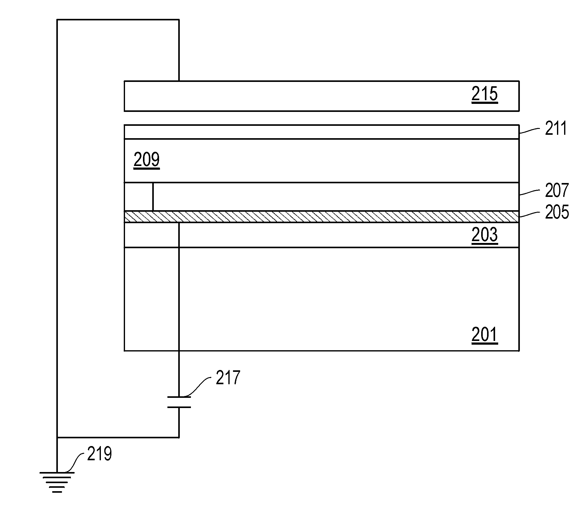
[0010]According to a first aspect, a Coulombic electrostatic chuck is provided that includes a substrate, a conductive layer overlying the substrate, and an arc elimination layer overlying the conductive layer. The electrostatic chuck further includes a high-k dielectric layer overlying the arc elimination layer, wherein the high-k dielectric layer has a dielectric constant of not less than about 10 and a resistivity of not less than about 1011 Ohm-cm.
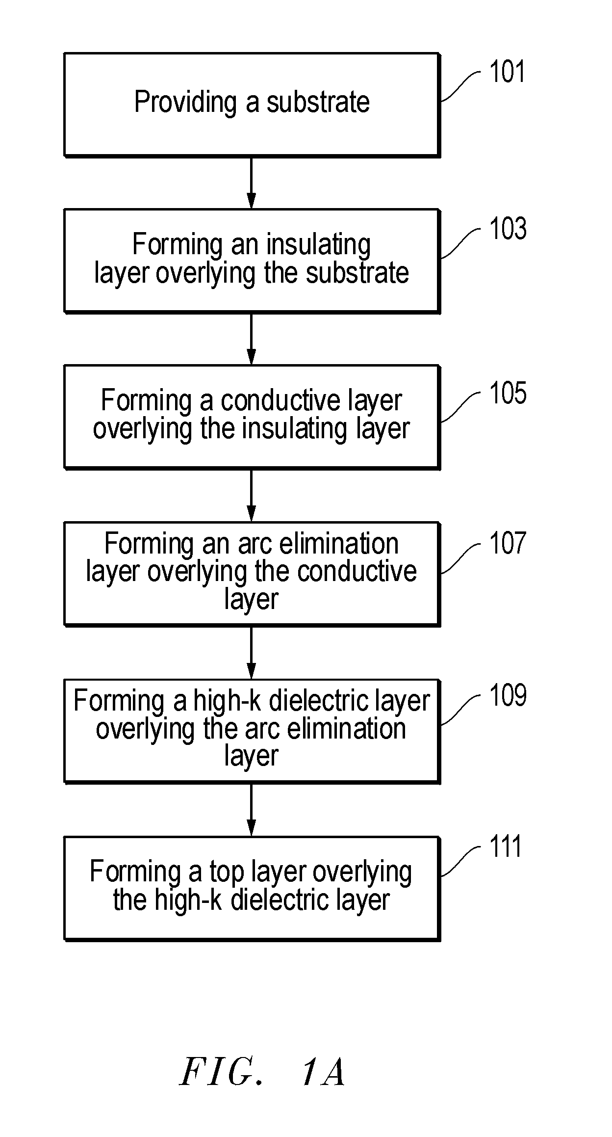
[0011]According to another aspect, a method is provided for forming a Coulombic electrostatic chuck, the method includes providing a substrate, forming a conductive layer made of a conductive material overlying the substrate, and forming an arc elimination layer overlying the conductive layer. The method further includes forming a high-k dielectric layer overlying the arc elimination layer, wherein the high-k dielectric layer has a diele

Problems solved by technology

Mechanical chucks have a disadvantage in that they often cause distortion of workpieces due to non-uniform forces being applied to the wafers.
Thus, wafers are often chipped or otherwise damaged, resulting in a lower yield.
In this respect, pressures in the chamber during semiconductor manufacturing processes tend to be low, and sufficient force cannot always be applied.
This shift to processing of larger workpieces, generally within high temperature and corrosive processing environments, places further demands on ESCs used during processing.

Method used


Image

  • Electrostatic chuck and method of forming
  • Electrostatic chuck and method of forming
  • Electrostatic chuck and method of forming

Examples


Embodiment Construction

)

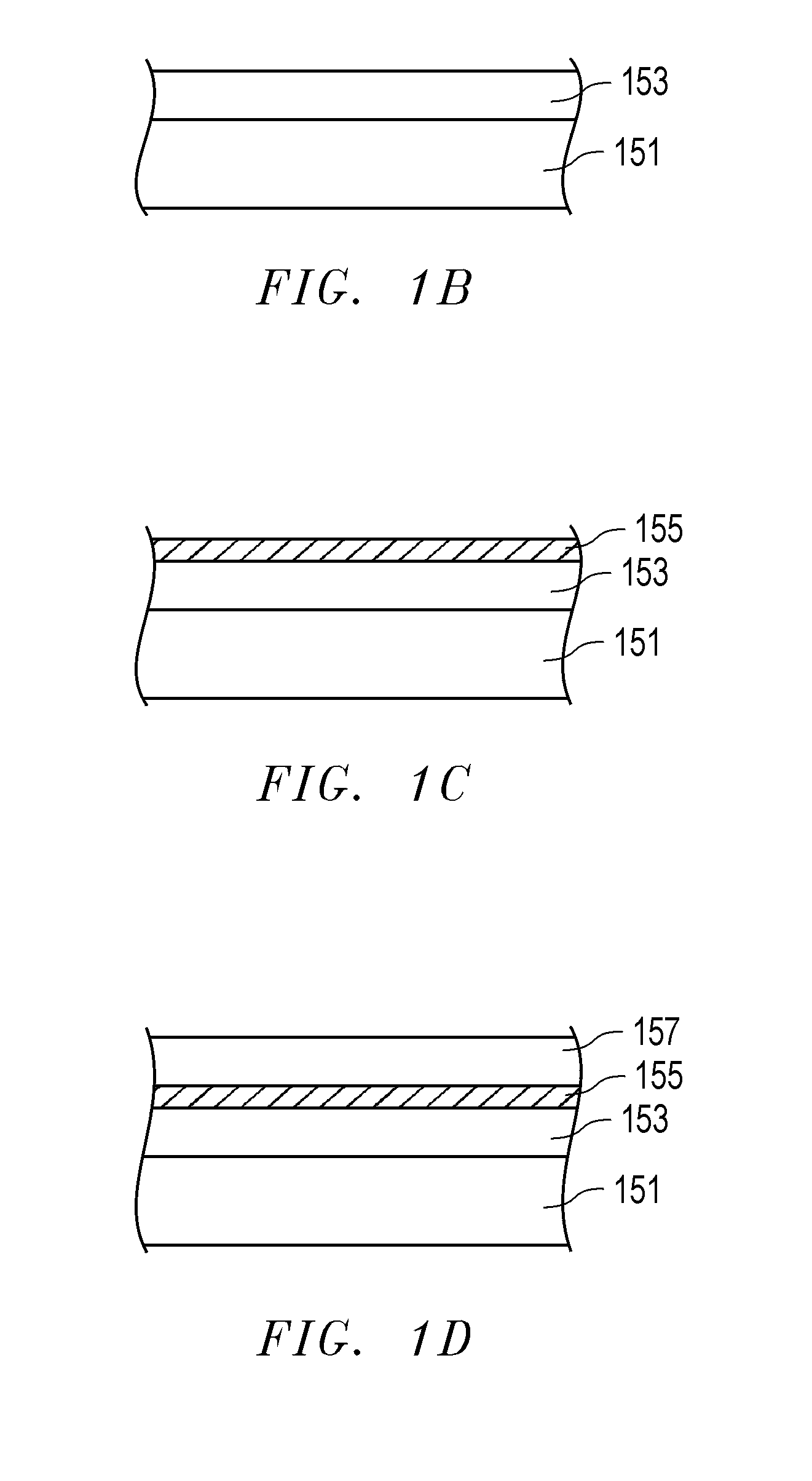
[0023]Referring to FIGS. 1A through 1F, a method according to an embodiment is initiated at step 101 by providing a substrate 151 suitable for forming overlying layers thereon. Suitable materials for the substrate 151 generally include inorganic materials. Such inorganic materials can include single crystalline, polycrystalline, or amorphous inorganic materials including for example, ceramics, glass-ceramics, and glasses. According to a particular embodiment, the substrate includes an insulating material, such as oxide-based materials. Suitable oxide-based materials can include aluminum oxide or silicon oxide, and are formed from a composition containing a majority of alumina oxide or silicon oxide. Such materials may be complex oxides or multiphase materials.

[0024]Other suitable inorganic materials for the substrate 151 can include metals and metal alloys. Suitable metals generally include aluminum, ferrous metals, or combinations thereof. In such embodiments utilizing a metal-con...


PUM

PropertyMeasurementUnit
Thicknessaaaaaaaaaa
Thicknessaaaaaaaaaa
Electrical resistanceaaaaaaaaaa

Abstract

A Coulombic electrostatic chuck is disclosed which includes a substrate, a conductive layer overlying the substrate, and an arc elimination layer overlying the conductive layer. The electrostatic chuck further includes a high-k dielectric layer overlying the arc elimination layer, wherein the high-k dielectric layer has a dielectric constant of not less than about 10 and a resistivity of not less than about 1011 Ohm-cm.

Description

CROSS-REFERENCE TO RELATED APPLICATION(S)[0001]The present application claims priority from U.S. Provisional Patent Application No. 60 / 871,882, filed Dec. 26, 2006, entitled “ELECTROSTATIC CHUCK AND METHOD OF FORMING”, naming inventor Matthew A. Simpson, which application is incorporated by reference herein in its entirety.BACKGROUND[0002]1. Field of the Disclosure[0003]This disclosure is directed to an electrostatic chuck (ESC) and is particularly directed to electrostatic chucks for use in processing of display panels.[0004]2. Description of the Related Art[0005]Chucks are used to support and hold wafers and substrates in place within high temperature and corrosive processing chambers such as those used for chemical vapor deposition, physical vapor deposition, or etching. Several main types of chucks have been developed. Mechanical chucks stabilize wafers on a supporting surface by using mechanical holders. Mechanical chucks have a disadvantage in that they often cause distortion ...

Claims


Application Information

Patent Timeline
IPC IPC(8): H02N3/00H01R43/00
CPCH01L21/6833Y10T29/49117Y10T279/23H02N13/00
Inventor SIMPSON, MATTHEW A.
Owner SAINT GOBAIN CERAMICS & PLASTICS INC
Learn More