
Method and apparatus for protection against process-induced charging

Active Publication Date: 2008-06-26
CYPRESS SEMICONDUCTOR
View PDF16 Cites 13 Cited by
  • Summary
  • Abstract
  • Description
  • Claims
  • Application Information

AI Technical Summary

Benefits of technology

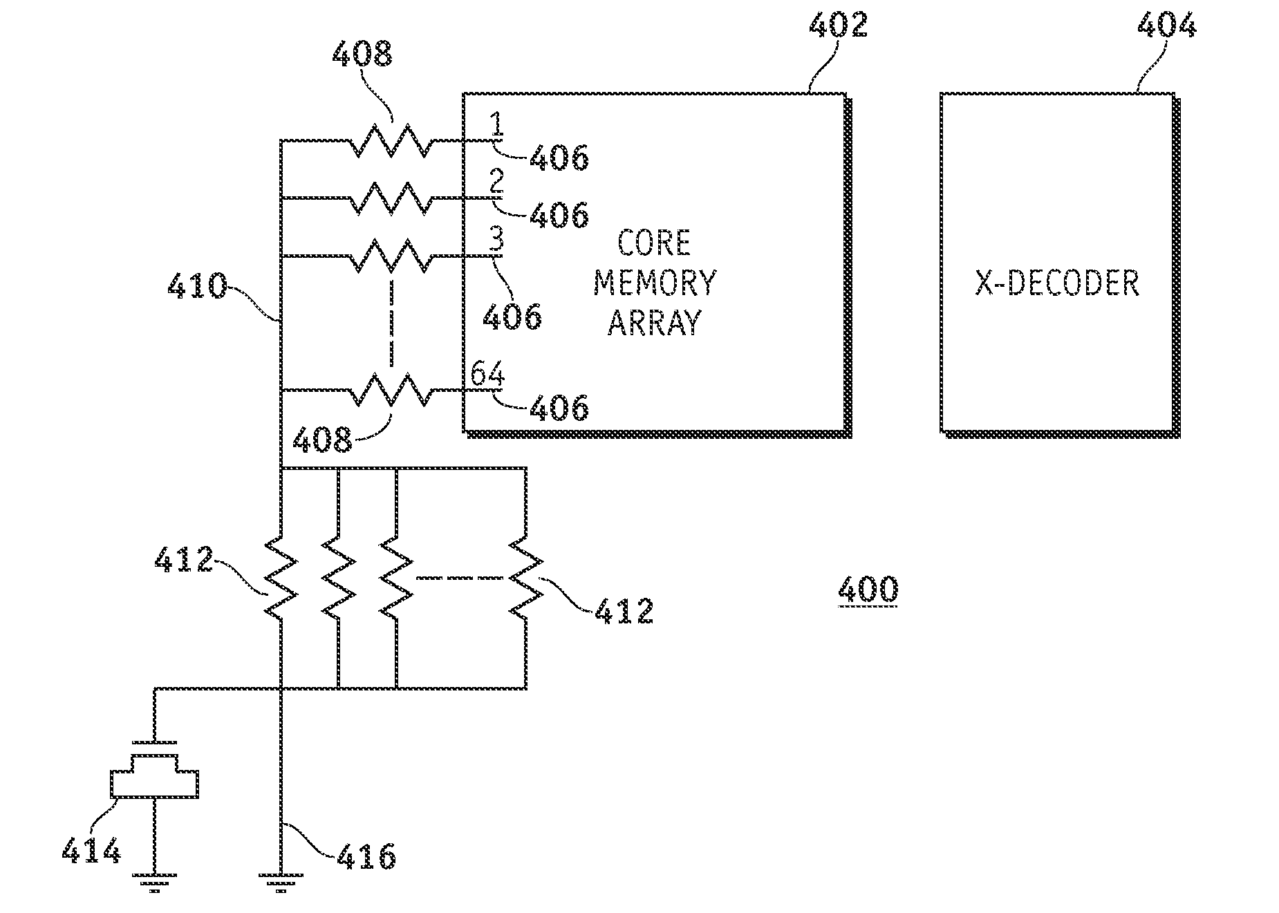
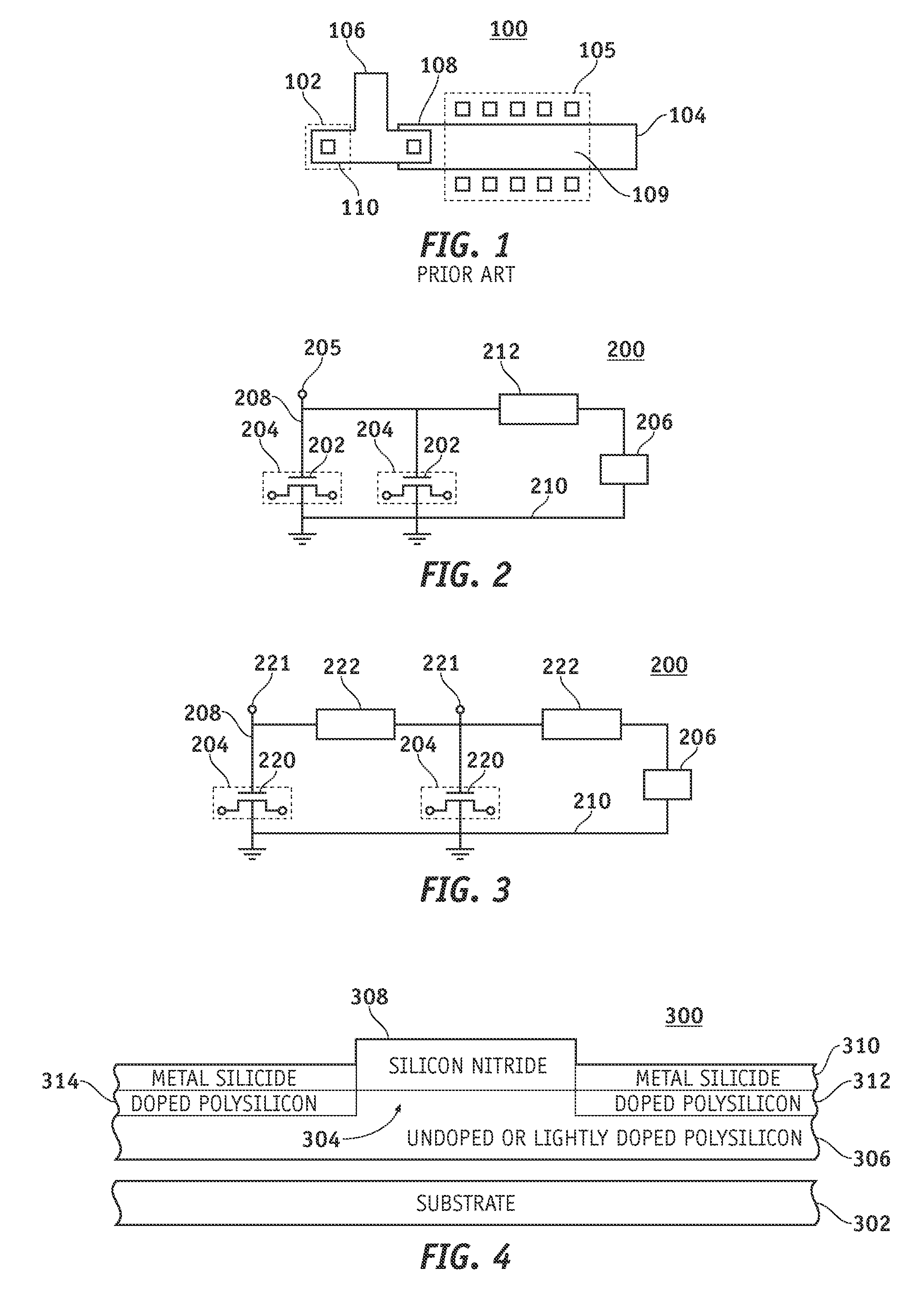
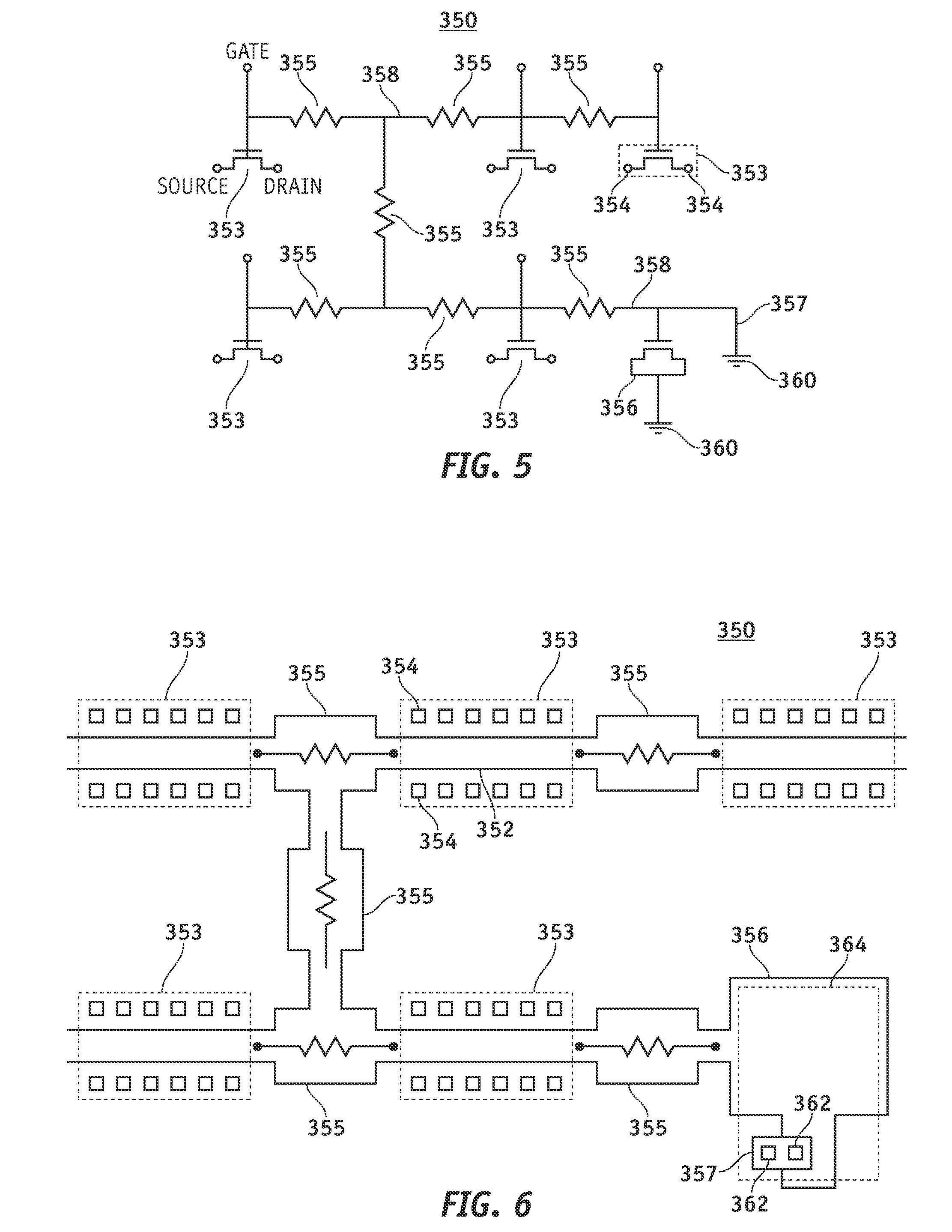
[0005]A semiconductor device for improved charge dissipation protection includes a substrate, a layer of semiconductive or conductive material, one or more thin film devices and a charge passage device. The thin film devices are connected to the semiconductive/conductive layer and the charge passage device is coupled to the thin film devices and to the substrate and provides a connection from the thin film devices to the substrate to dissipate charge from the semiconductive/conductive layer to the substrate.
[0006]A method for forming a sem

Problems solved by technology

In-process charging of gate electrodes in insulated gate field effect transistors (IGFETs) can damage the gate dielectrics of the transistors.
In a MOSFET, the in-process charging of the gate causes large voltages and large electric fields to occur across the gate dielectric of the MOSFET.
Large electric fields across the gate dielectric can cause small tunneling currents to flow through the dielectric and the tunneling currents can leave charge trapped in the dielectric.
Gate dielectric charging and gate to substrate or gate to well breakdown can each result in product failure.

Method used


Image

  • Method and apparatus for protection against process-induced charging
  • Method and apparatus for protection against process-induced charging
  • Method and apparatus for protection against process-induced charging

Examples


Embodiment Construction

[0045]The following detailed description of the invention is merely exemplary in nature and is not intended to limit the invention or the application and uses of the invention. Furthermore, there is no intention to be bound by any theory presented in the preceding background of the invention or the following detailed description of the invention.

[0046]Before describing in detail embodiments that are in accordance with the present invention, it should be observed that the embodiments reside primarily in combinations of method steps and apparatus components related to protection against process-induced charges. Accordingly, the apparatus components and method steps have been represented where appropriate by conventional symbols in the drawings, showing only those specific details that are pertinent to understanding the embodiments of the present invention so as not to obscure the disclosure with details that will be readily apparent to those of ordinary skill in the art having the ben...


PUM


Abstract

A semiconductor device (400) for improved charge dissipation protection includes a substrate (426), a layer of semiconductive or conductive material (406), one or more thin film devices (408) and a charge passage device (414). The thin film devices (408) are connected to the semiconductive or conductive layer (406) and the charge passage device (414) is coupled to the thin film devices (408) and to the substrate (426) and provides a connection from the thin film devices (408) to the substrate (426) to dissipate charge from the semiconductive / conductive layer (406) to the substrate (426).

Description

FIELD OF THE DISCLOSURE[0001]The present invention generally relates to semiconductor devices, and more particularly relates to a method and apparatus for protection of nodes of sensitive semiconductor devices against process-induced charging.BACKGROUND OF THE DISCLOSURE[0002]In-process charging of gate electrodes in insulated gate field effect transistors (IGFETs) can damage the gate dielectrics of the transistors. In the most common form of IGFET, the modern MOSFET (metal-oxide-semiconductor field-effect transistor), the gate electrode is formed from polysilicon. In a MOSFET, in-process charging commonly occurs during the etching of the MOSFET's polysilicon gate. Charging of a polysilicon gate can also occur during the processing of layers subsequent to the processing of the polysilicon gate when those subsequent layers are electrically connected to the polysilicon gate. These subsequent layers are typically contact layers, other polysilicon layers and metal layers.[0003]In a MOSF...

Claims


Application Information

Patent Timeline
IPC IPC(8): H01L23/60G11C5/00
CPCG11C8/08G11C8/14H01L27/0248H01L2924/0002H01L29/66477H01L2924/00H01L21/768
Inventor ROGERS, DAVID M.QIAN, MIMI X.APPIAH, KWADWO A.RANDOLPH, MARKVANBUSKIRK, MICHAEL A.KAMAL, TAZRIENKINOSHITA, HIROYUKIHE, YIZHENG, WEI
Owner CYPRESS SEMICONDUCTOR
Features
  • Generate Ideas
  • Intellectual Property
  • Life Sciences
  • Materials
  • Tech Scout
  • Unparalleled Data Quality
  • Higher Quality Content
  • 60% Fewer Hallucinations
Learn More