

LEAKAGE BARRIER FOR GaN BASED HEMT ACTIVE DEVICE
a technology of active devices and leakage barriers, which is applied in the direction of basic electric elements, semiconductor devices, electrical equipment, etc., can solve the problems of poor electrical isolation between the source and gate, poor leakage current and inapplicability of gan based materials insulated gate techniques
- Summary
- Abstract
- Description
- Claims
- Application Information
AI Technical Summary
Benefits of technology
Problems solved by technology
Method used
Image

Examples
Embodiment Construction
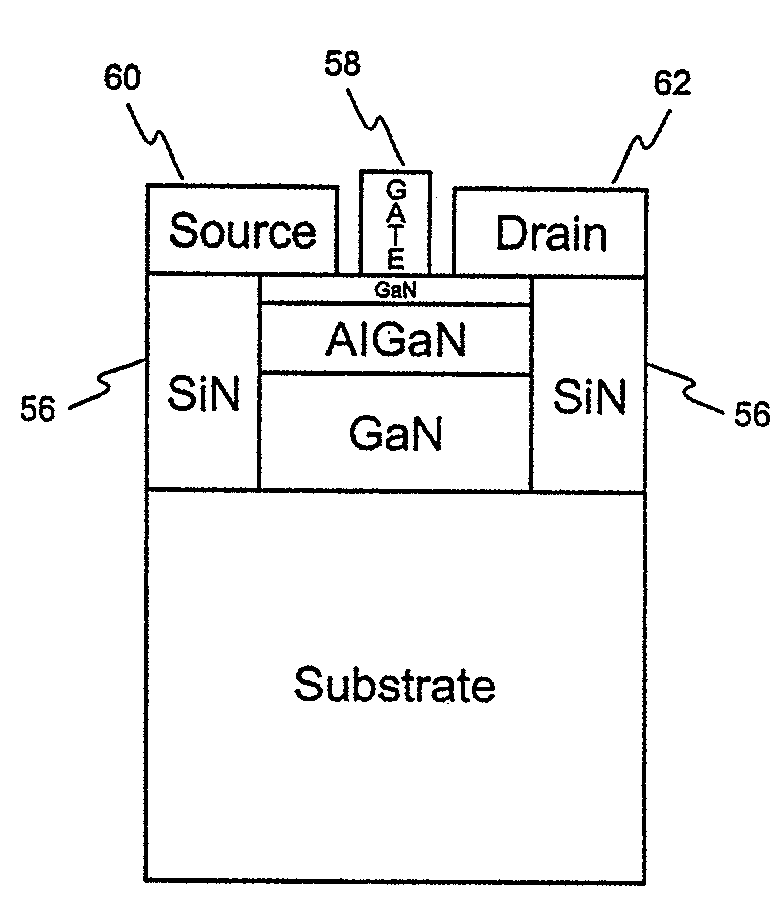
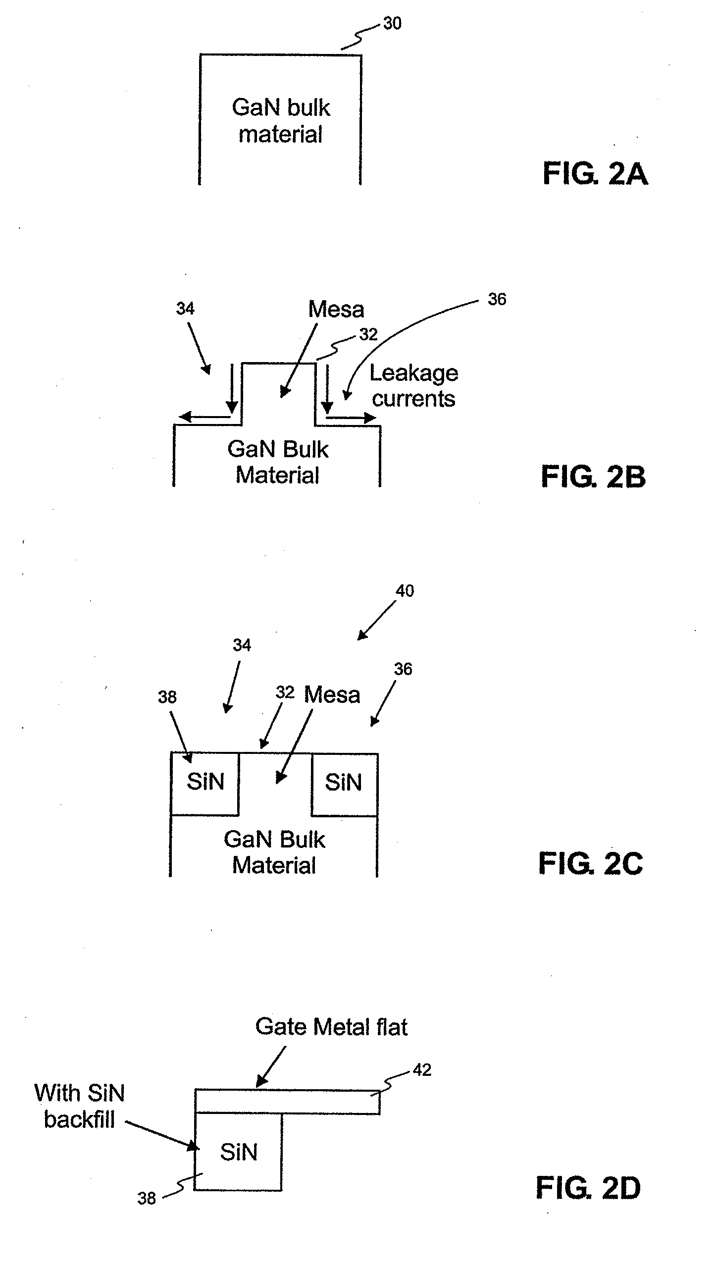
[0018]The present invention relates to a HEMT formed from a GaN material system which has relatively less leakage current than known HEMTs formed from GaN material systems and also solves the problem of current constriction of the gate metal. Two embodiments of the invention are disclosed. One embodiment, illustrated in FIGS. 2A-2D, relates to an embodiment of the invention in which the HEMT is formed from bulk GaN material. An alternate embodiment of the invention is illustrated in FIGS. 3A-3F in which the HEMT is formed from GaN / AlGaN.
[0019]Referring to FIGS. 2A-2D, a simplified explanation of the process in accordance with one embodiment of the present invention is provided. Referring first to FIG. 2A, a bulk GaN material 30 may be used as the starting point for the HEMT. The bulk GaN material is masked by convention photolithography techniques and etched, for example, by buffered oxide wet or Cl-based dry etching, to form a mesa 32. The gate mesa 32 defines a pair of step discon...
PUM
 Abstract
Description
Claims
Application Information