

Semocondutor device having multiple-layer hard mask with opposite stresses and method for fabricating the same
a technology of a semiconductor device and a hard mask, which is applied in the direction of semiconductor devices, semiconductor/solid-state device details, electrical apparatus, etc., can solve the problems of peeling event and limit of the use of multiple-layer structures, and achieve the effect of reducing peeling even
- Summary
- Abstract
- Description
- Claims
- Application Information
AI Technical Summary
Benefits of technology
Problems solved by technology
Method used
Image

Examples
Embodiment Construction
[0015]Embodiments of the present invention relate to a semiconductor device having a multiple-layer hard mask with opposite stresses and a method for fabricating the same.
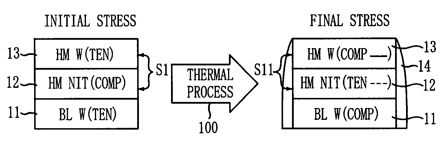
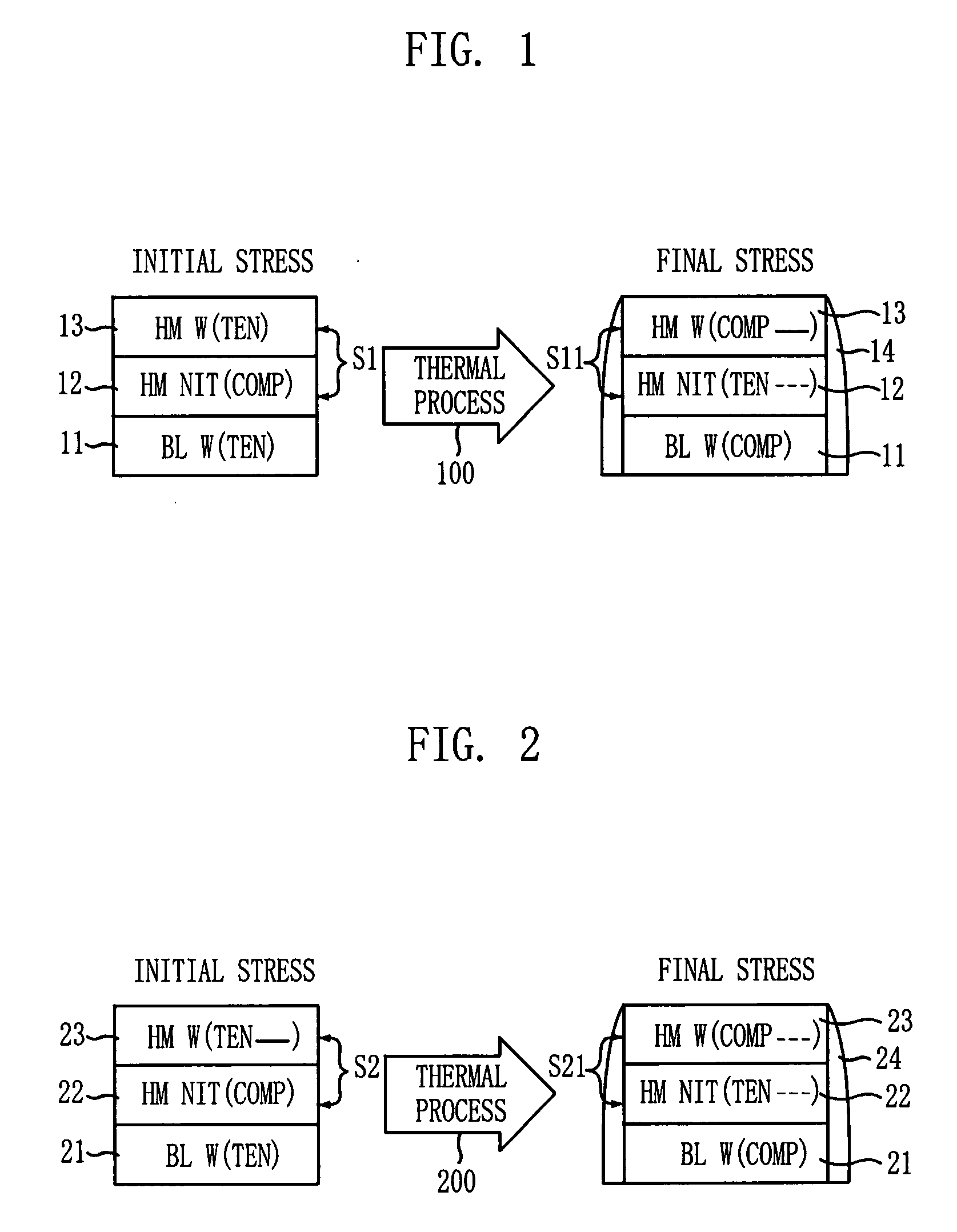
[0016]FIG. 2 illustrates a diagram showing a structure of a pattern using a multiple-layer hard mask in accordance with an embodiment of the present invention. A first hard mask 22 is formed over a tungsten (W) layer 21. A second hard mask 23 is formed over the first hard mask 22. The tungsten layer 21 functions as a bit line and is denoted as ‘BL W’. The first hard mask 22 may include a nitride-based layer and is denoted as ‘HM NIT’. The second hard mask 23 may include a tungsten layer and is denoted as ‘HM W’.
[0017]An initial stress after formation for the tungsten layer 21 and the second hard mask 23 is a tensile stress (TEN), and for the first hard mask 22 is a compressive stress (COMP).
[0018]In this embodiment of the present invention, the initial stress of the second hard mask 23, which is formed at the top, ...
PUM
 Abstract
Description
Claims
Application Information