Sapphire substrates and methods of making same

a technology of substrates and nitride, applied in the field of saphire substrates, can solve the problems of lattice mismatch, difficulty in producing boules and substrates of such nitride semiconducting materials, and difficulty in producing high-quality substrates in larger sizes

Inactive Publication Date: 2008-07-10
SAINT GOBAIN CERAMICS & PLASTICS INC
View PDF27 Cites 262 Cited by
  • Summary
  • Abstract
  • Description
  • Claims
  • Application Information

AI Technical Summary

Benefits of technology

[0008]One embodiment is drawn to a sapphire substrate including a generally planar surface having a crystallographic orientation selected from the group consisting of a-plane, r-plane, m-plane, and c-plane orientatio...

Problems solved by technology

However, manufacturing boules and substrates of such nitride semiconducting materials has proven difficult for a multitude of reasons.
Such foreign substrates have a different crystal lattice structure than nitride semiconducting materials, particularly GaN, and thus have a lattice mismatch.
Despite s...

Method used


Image

  • Sapphire substrates and methods of making same
  • Sapphire substrates and methods of making same
  • Sapphire substrates and methods of making same

Examples


examples

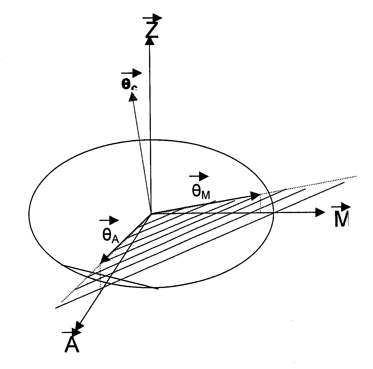
[0077]The following examples provide methods for processing wafers according to several embodiments, and particularly describe processing parameters for production of high surface area wafers having improved dimensional qualities and orientations. In the following examples, c-plane sapphire wafers having diameters of 2 inches, 3 inches, and 4 inches were processed and formed in accordance with embodiments provided herein.

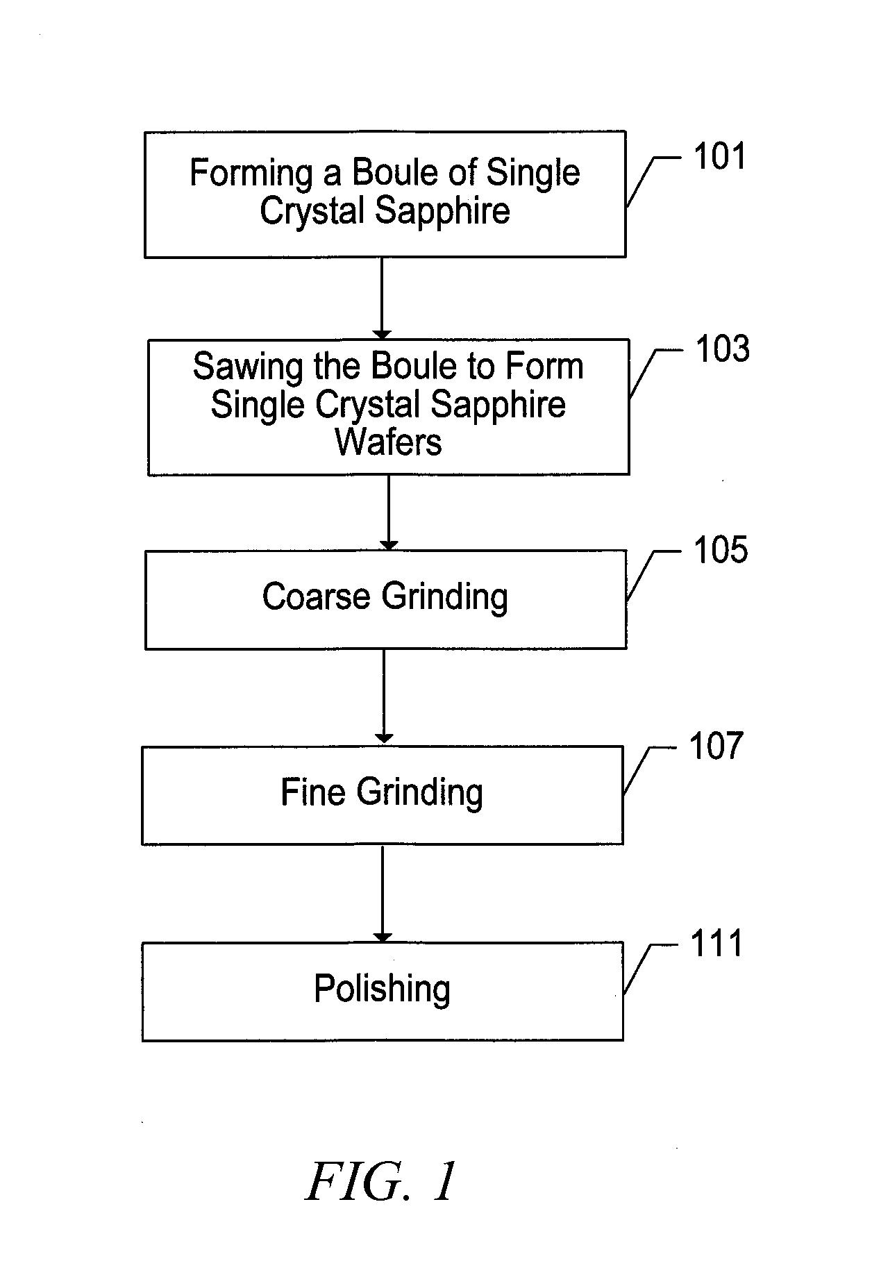
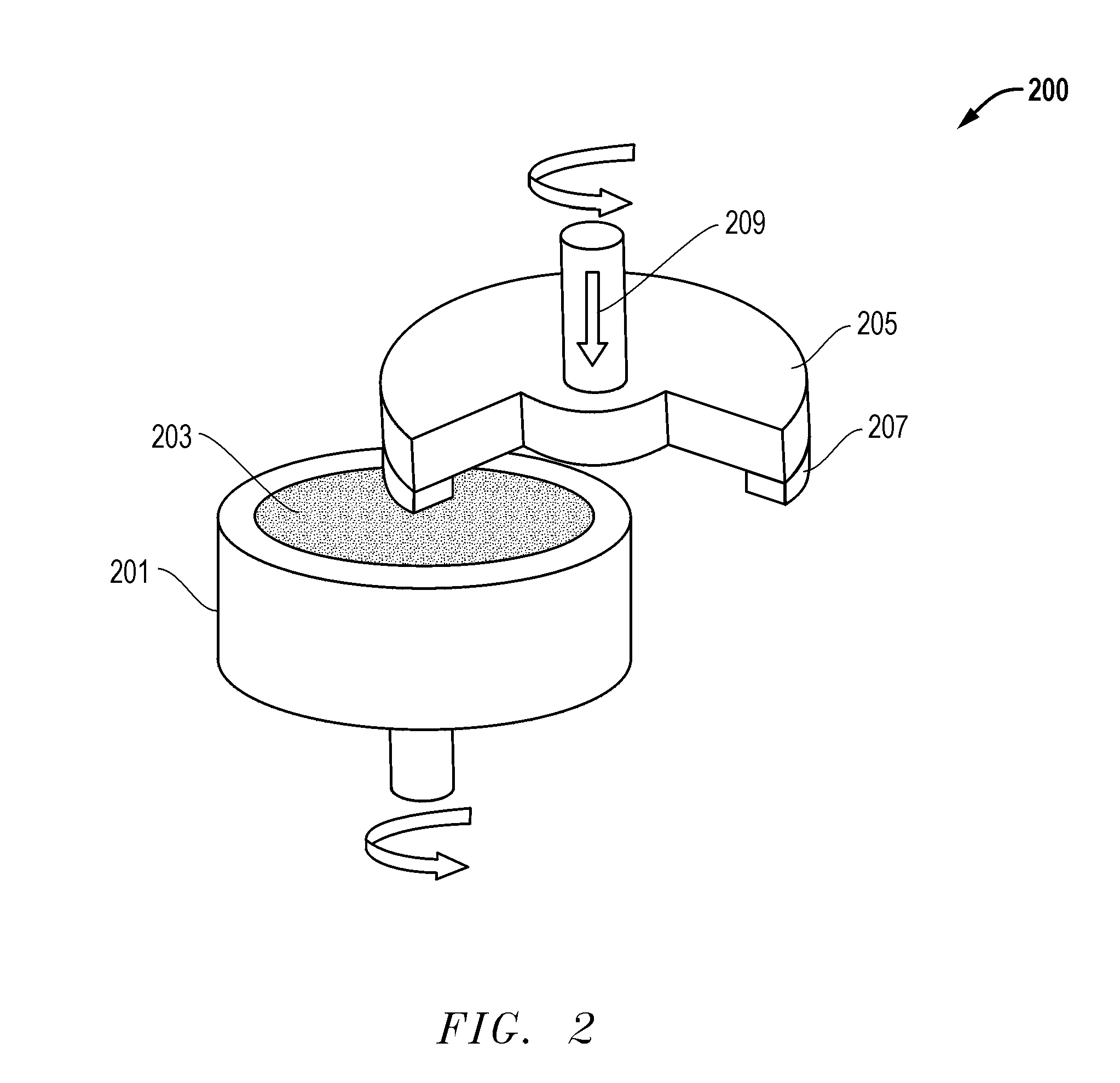
[0078]Processing initiates with a boule that is sectioned or sliced, as described above. The boule is sectioned using a wire sawing technique, wherein the boule is placed and rotated over wires coated with cutting elements, such as diamond particles. The boule is rotated at a high rate of speed, within a range of between about 2000 rpm and 5000 rpm. While the boule is rotating it is in contact with multiple lengths of wiresaw, which are typically reciprocated at a high speed in a direction tangential to the surface of the boule, to facilitate slicing. The lengths of...


PUM


Abstract

A sapphire substrate includes a generally planar surface having a crystallographic orientation selected from the group consisting of a-plane, r-plane, m-plane, and c-plane orientations, and having a nTTV of not greater than about 0.037 μm/cm2, wherein nTTV is total thickness variation normalized for surface area of the generally planar surface, the substrate having a diameter not less than about 9.0 cm.

Description

CROSS-REFERENCE TO RELATED APPLICATION(S)[0001]The present application claims priority from U.S. Provisional Patent Application No. 60 / 882,343, filed Dec. 28, 2006, entitled “SAPPHIRE SUBSTRATES AND METHODS OF MAKING SAME”, naming inventors Brahmanandam V. Tanikella, Matthew A. Simpson, Palani Chinnakaruppan, Robert A. Rizzuto, Isaac K. Cheman, and Rama Vedantham, which application is incorporated by reference herein in its entirety.BACKGROUND[0002]1. Field of the Disclosure[0003]The present application is generally directed to sapphire substrates and methods of finishing such substrates.[0004]2. Description of the Related Art[0005]Semiconducting components based on single crystal nitride materials of Group-III and Group-V elements are ideal for devices such as light-emitting diodes (LED), laser diodes (LD), displays, transistors and detectors. In particular, semiconductor elements utilizing Group-III and Group-V nitride compounds are useful for light emitting devices in the UV and ...

Claims


Application Information

Patent Timeline
IPC IPC(8): H01L31/036
CPCC30B29/20B28D5/00
Inventor TANIKELLA, BRAHMANANDAM V.SIMPSON, MATTHEW A.CHINNAKARUPPAN, PALANIAPPANRIZZUTO, ROBERT A.CHERIAN, ISAAC K.VEDANTHAM, RAMANUJAM
Owner SAINT GOBAIN CERAMICS & PLASTICS INC
Why Eureka
Try Eureka