Vertical cavity surface emitting laser diode

a laser diode and vertical cavity technology, applied in semiconductor lasers, optical resonator shape and construction, laser details, etc., can solve the problems of increased error or limitation in transmission bands, difficult to make control of polarization direction of vertical cavity surface emitting laser diodes, and difficult to perform, etc., to achieve high performance, controllability of polarization mode and/or mass productivity

Inactive Publication Date: 2006-08-24
KK TOSHIBA
View PDF3 Cites 36 Cited by
  • Summary
  • Abstract
  • Description
  • Claims
  • Application Information

AI Technical Summary

Benefits of technology

[0021] The present invention has been made in view of these circumstances and an object thereof is to provide a vertical cavity surface emitting laser diode with high performance where controllability i

Problems solved by technology

As regards the polarization mode, however, it is difficult to make control on a polarization direction in the vertical cavity surface emitting laser diode, as compared with the end face emitting laser diode.
This is due to symmetry in (100) plane substrate used for manufacturing an ordinary vertical cavity surface emitting laser diode or a device structure itself, and because linear polarization can be obtained but there is no gain difference between orthogonal polarized waves in the active region itself and it is difficult to perform such measure as increasing a reflectivity of a reflecting mirror to a polarized wave in a specific orientation.
Even when ordinary data communication is performed, instability of the polarization mode causes over-noise mode competition and also causes such a problem as increase in error or limitation in transmission band.
Since the reflectivity of the mirror to polarized lights parallel to the metal wires becomes high, it is effective for stabilizing a polarization plane to some extent, but there is difficulty in manufacture because it is necessary to form metal wires with a width equal to or less than a light wavelength.
The stress (strain)-applying region or the asymmetrical mesa structure includes such a problem that device processing is co

Method used


Image

  • Vertical cavity surface emitting laser diode
  • Vertical cavity surface emitting laser diode
  • Vertical cavity surface emitting laser diode

Examples


first embodiment

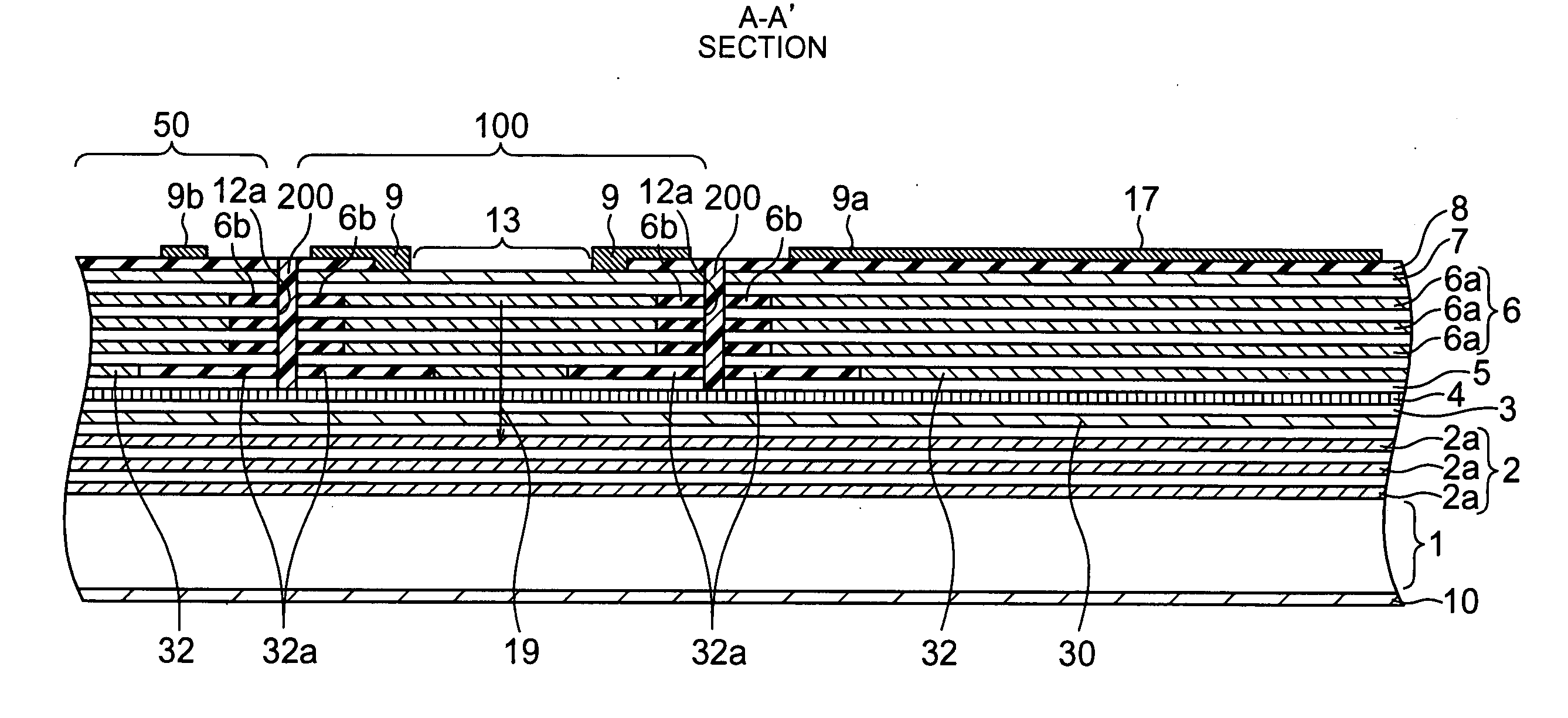
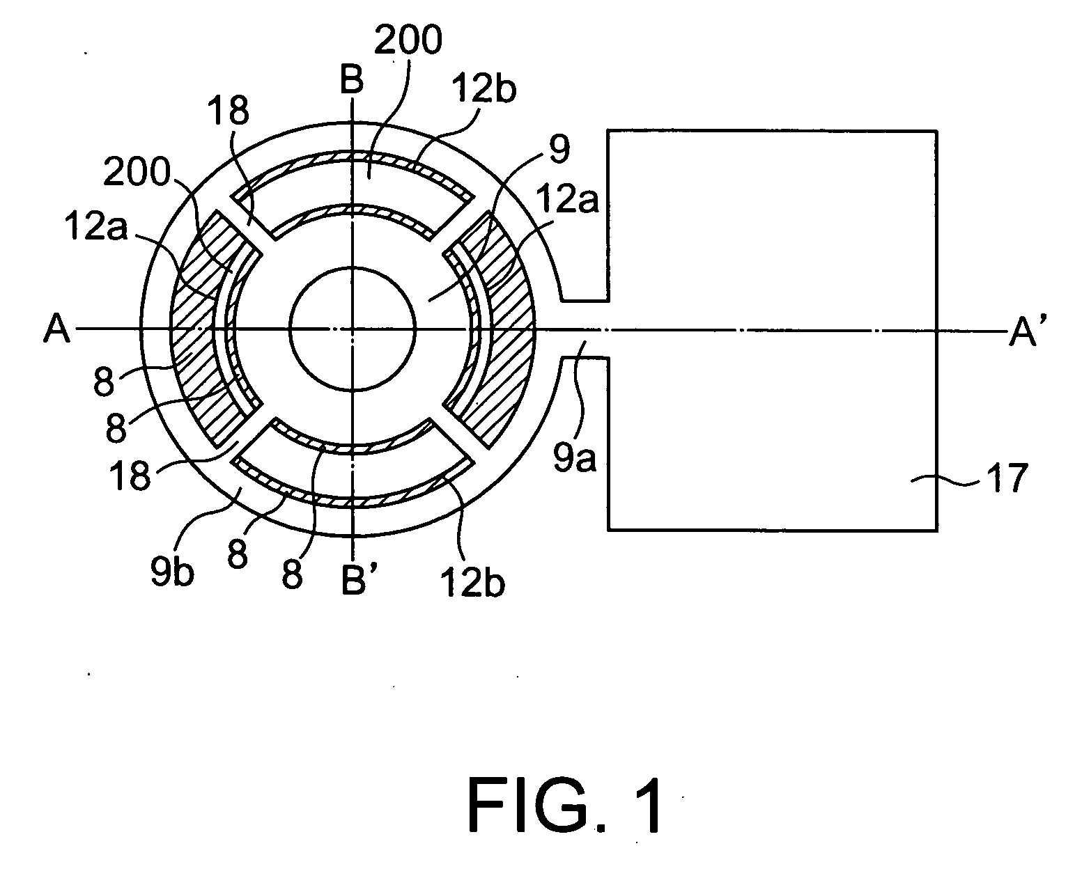
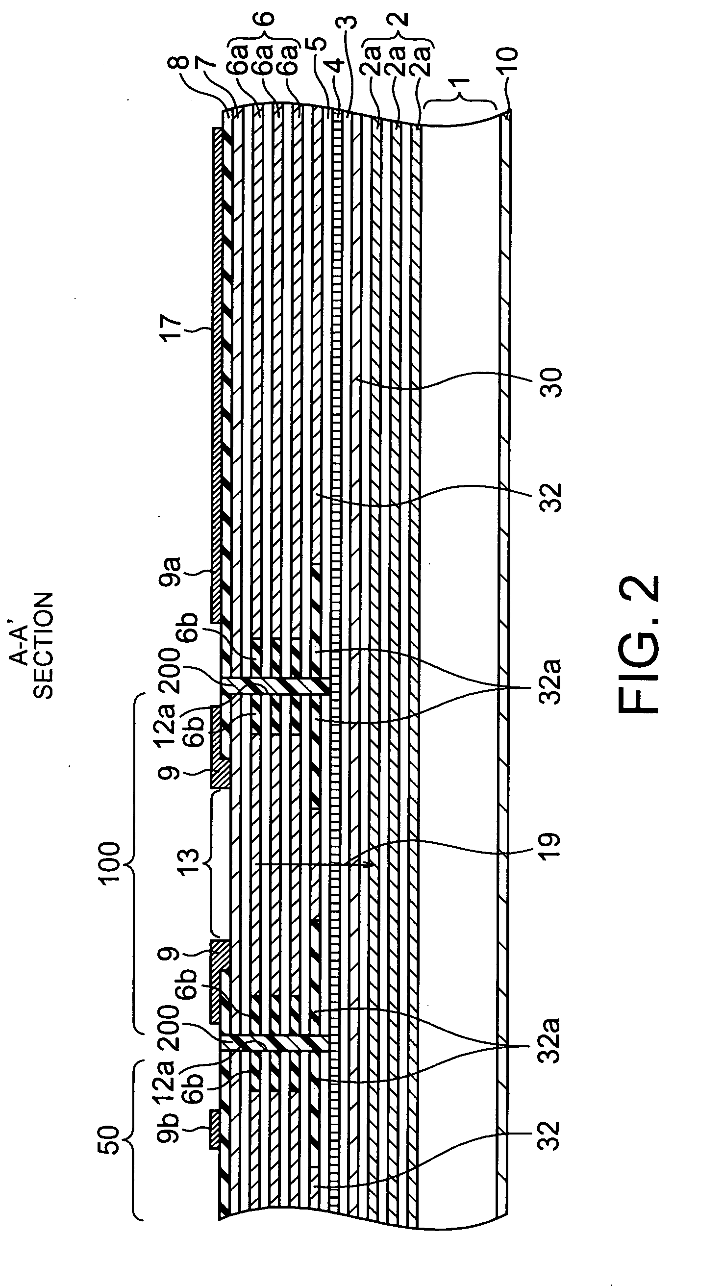
[0084] FIGS. 1 to 9 are illustrative views showing a structure of a vertical cavity surface emitting laser diode according to a first embodiment of the present invention. FIG. 1 is a plan view of the vertical cavity surface emitting laser diode, FIG. 2 is a sectional view of the vertical cavity surface emitting laser diode taken along A-A′ shown in FIG. 1, and FIG. 3 is a sectional view of the vertical cavity surface emitting laser diode taken along B-B′ shown in FIG. 1. FIG. 4 is a view showing a shape of an oxidized region 32a of an upper to-be-oxidized layer 32 obtained when the vertical cavity surface emitting laser diode has been cut at a height 26 thereof (see FIG. 5), FIG. 5 is a sectional view of the vertical cavity surface emitting laser diode taken along line A-A′ shown in FIG. 4, and FIG. 6 is a sectional view of the vertical cavity surface emitting laser diode taken along line B-B′ shown in FIG. 4. FIG. 7 is a view showing a shape of an oxidized layer of a lower to-be-ox...

example

[0110] Next, the method for manufacturing a vertical cavity surface emitting laser diode according to the first embodiment will be specifically explained as examples.

[0111] First, an n-type semiconductor multi-layer film reflecting mirror 2, a to-be-oxidized layer 30 for forming a current confinement portion, a cladding layer 3, a semiconductor active layer 4, a cladding layer 5, a to-be-oxidized layer 32 for forming the current confinement portion, a p-type semiconductor multi-layer film reflecting mirror 6, and a contact layer 7 were sequentially grown on a cleaned n-type GaAs substrate 1 with plane orientation (100) plane having 3-inch square and a thickness of 400 μm using a MOCVD (metal organic chemical vapor deposition) apparatus.

[0112] Here, assuming that a structure where the semiconductor multi-layer film reflecting mirrors 2 and 6 were disposed above and below an optical cavity constituted of the semiconductor active layer 4, and the cladding layers 3 and 5 was a basic s...

first modification

(First Modification)

[0127] Next, a vertical cavity surface emitting laser diode according to a first modification of the first embodiment will be explained with reference to FIGS. 10 to 12. FIG. 10 is a view showing a shape of an oxidized region 32a of an upper to-be-oxidized layer 32 of a vertical cavity surface emitting laser diode according to a first modification of the first embodiment obtained when the vertical cavity surface emitting laser diode has been cut at a height 26 (see FIG. 11) thereof, FIG. 11 is a sectional view of the vertical cavity surface emitting laser diode according to the first modification, taken along line A-A′ shown in FIG. 10, and FIG. 12 is a sectional view of the vertical cavity surface emitting laser diode according to the first modification, taken along line B-B′ shown in FIG. 10.

[0128] The vertical cavity surface emitting laser diode according to the first modification has such a constitution that the lower to-be-oxidized layer 30 is removed, size...


PUM


Abstract

It is made possible to obtain high performance having high controllability in polarization mode even when a vertical cavity surface emitting laser diode is fabricated on an ordinary substrate with a plane orientation (100) plane or the like. A vertical cavity surface emitting laser diode includes: a substrate; a semiconductor active layer which is formed on the substrate and has a light emitting region; a first reflecting mirror and a second reflecting mirror sandwiching the semiconductor active layer; a first recess which has a first groove depth penetrating at least the semiconductor active layer from the outermost layer of the first reflecting mirror; a second recess having a second groove depth shallower than the first groove depth; a mesa portion which is surrounded by the first and second recesses; and an insulating film which is buried in the first recess.

Description

CROSS-REFERENCE TO RELATED APPLICATION [0001] This application is based upon and claims the benefit of priority from prior Japanese Patent Application No. 2005-9092 filed on Jan. 17, 2005 in Japan, the entire contents of which are incorporated herein by reference. BACKGROUND OF THE INVENTION [0002] 1. Field of the Invention [0003] The present invention relates to a vertical cavity surface emitting laser (VCSEL) diode. [0004] 2. Related Art [0005] Semiconductor light emitting devices such as a laser diode or a semiconductor light emitting diode have been broadly used in not only an optical communication field but also such an optical disk system as a CD (compact disc) or a DVD (digital versatile disc), or a barcode reader. When the semiconductor light emitting devices are used in various application fields including such an optical communication field, it becomes important to unitize operation modes regarding three modes of “longitudinal mode”, “transverse mode”, and “polarization mo...

Claims


Application Information

Patent Timeline
IPC IPC(8): H01S3/08
CPCH01S5/18308H01S5/18311H01S5/18313H01S5/1833H01S5/18338H01S5/18355H01S5/2213H01S5/3202H01S2301/176H01S5/3201
Inventor EZAKI, MIZUNORIKUSHIBE, MITSUHIRONISHIGAKI, MICHIHIKOTAKAOKA, KEIJI
Owner KK TOSHIBA
Why Eureka
Try Eureka