

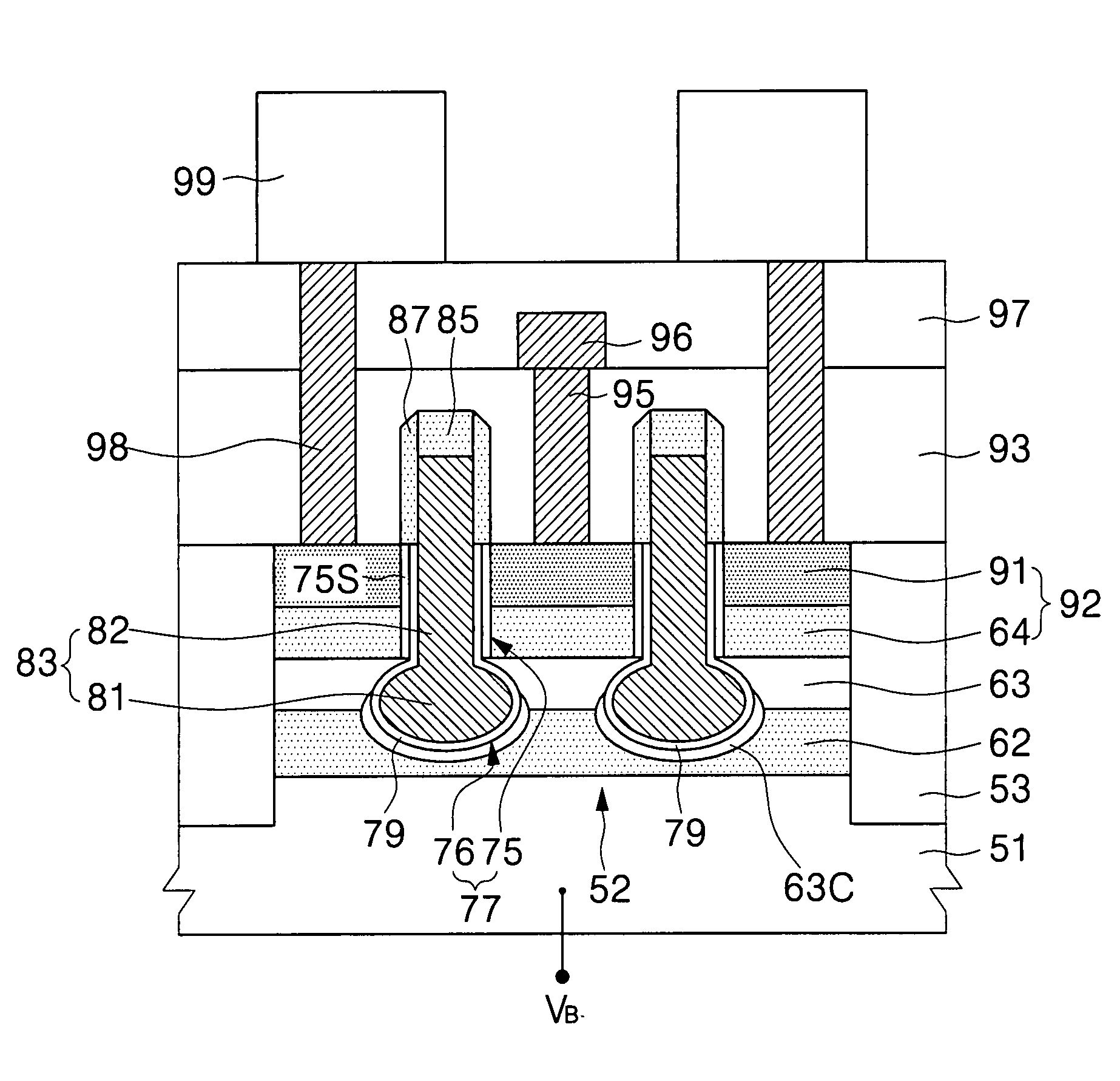
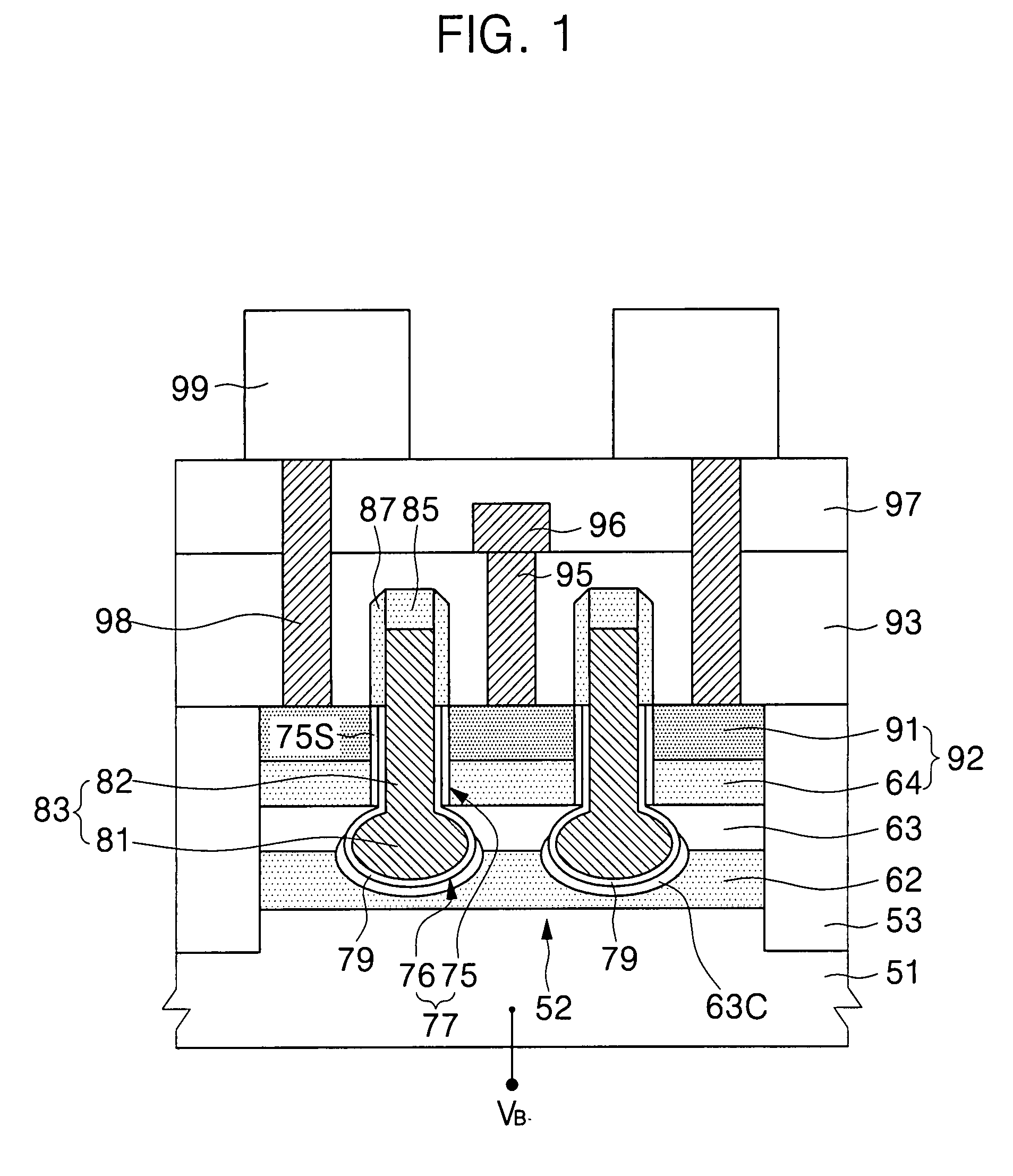
Semiconductor devices and dynamic random access memories having a retrograde region and methods of forming the same
a technology of dynamic random access memory and semiconductor devices, which is applied in the direction of liquid fuel feeders, mechanical equipment, machines/engines, etc., can solve the problems of exaggerating the threshold voltage, deteriorating refresh characteristics, and increasing off-current, so as to achieve the effect of increasing the threshold voltag
- Summary
- Abstract
- Description
- Claims
- Application Information
AI Technical Summary
Benefits of technology
Problems solved by technology
Method used
Image

Examples
examples
[0097]Table 1 shows the results of changes in threshold voltage due to a body effect in accordance with some embodiments of the present invention.
TABLE 1Change in threshold voltage due to body effectItemSample 1Sample 2P ion implantation0180 KV, 5E+12atoms / cm2Threshold voltage0.699 V0.683 VBE0.287 V / −1 V0.162 V / −1 V
[0098]In Table 1, Sample 1 and Sample 2 are fabricated to have a gate length of 35 nm, a gate width of 50 nm, and a gate trench depth of 180 nm. A phosphorus ion implantation process for forming a retrograde region is performed on Sample 2, and is not performed on Sample 1. The phosphorus ion implantation process for forming a retrograde region is performed on Sample 2 at an energy of 180 KV and a dose of 5E+12 atoms / cm2
[0099]Referring to Table 1, threshold voltages of Sample 1 and Sample 2 are 0.699V and 0.683V, respectively. That is, it can be found that the threshold voltages of Sample 1 and Sample 2 have similar levels to each other. The threshold voltage change rate...
PUM
 Abstract
Description
Claims
Application Information