Etch resist solution, method of fabricating thin film pattern using the same and method of fabricating an LCD device using the same

Active Publication Date: 2008-07-24
LG DISPLAY CO LTD
View PDF7 Cites 55 Cited by
  • Summary
  • Abstract
  • Description
  • Claims
  • Application Information

AI Technical Summary

Benefits of technology

[0022]An advantage of the present invention is to provide an etch resist solution, a method of fabricating a thin film pattern and a method of fabricating an LCD device, in which the life of a blanket is improved so that fabrication costs may be reduced and fabrication reliability may be improved.
[0023]Additional features and advantages of the invention will be set forth in part in the description which follows, and in part will be apparent from the description, or may be learned by practice of the invention. These and other advantages of the invention will be realized and attained by the composition and methods particularly pointed out in the written description and claims hereof as well as the appended drawings.
[0024]To achieve these and other advantages and in accordance with the purpose of the present invention, as embodied and broadly described, an etch resist solution includes a base polymer; a printing solvent that satisfies the condition 6>δsolvent or δsolvent>11, where δsolvent is the solubility parameter of the solvent, or satisfies the condition 6<δsolvent<11 and μ<2(D), where μ is the dipole moment; a carrier solvent; and a surfactant.
[0025]In another aspect of the present invention, a method of fabricating a thin film pattern includes injecting an etch resist solution into a blanket on a printing roller, wherein the etch resist solution includes a printing solvent that satisfies the condition 6>δsolvent or δsolvent>11, where δsolvent is the solubility parameter of the solvent, or satisfies the condition 6<δsolvent<11 and μ<2(D), where μ is the dipole moment of the solvent; rotating the printing roller to uniformly coat the etch resist solution on the blanket; rolling the

Problems solved by technology

These processes increase the fabricating cost of the liquid crystal

Method used


Image

  • Etch resist solution, method of fabricating thin film pattern using the same and method of fabricating an LCD device using the same
  • Etch resist solution, method of fabricating thin film pattern using the same and method of fabricating an LCD device using the same
  • Etch resist solution, method of fabricating thin film pattern using the same and method of fabricating an LCD device using the same

Examples


Example

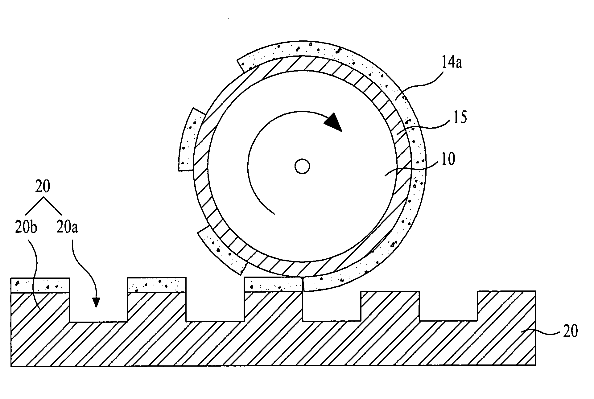
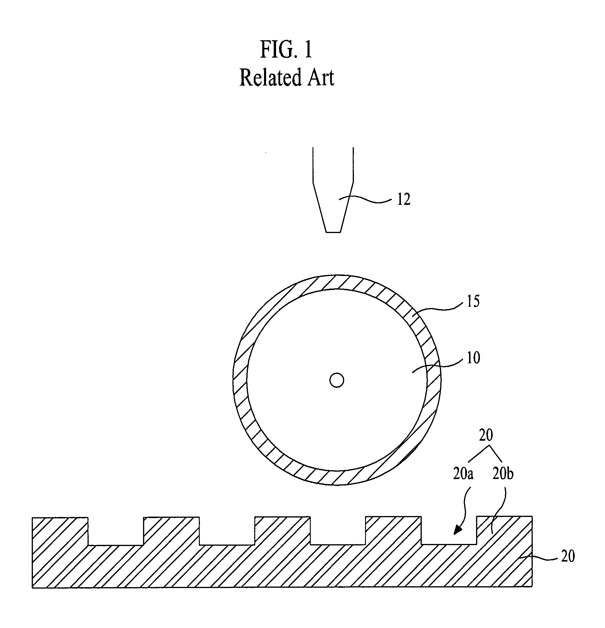
[0033]Reference will now be made in detail to embodiments of the present invention, examples of which are illustrated in the accompanying drawings. Wherever possible, the same reference numbers will be used throughout the drawings to refer to the same or similar parts.

[0034]An apparatus and method of fabricating a thin film pattern according to an embodiment of the present invention may utilize an etch resist solution that does not damage a blanket on a printing roll. The etch resist solution is used to form a thin film pattern. Thereby, reliability of the thin film pattern is improved and at the same time the life of the blanket is improved.

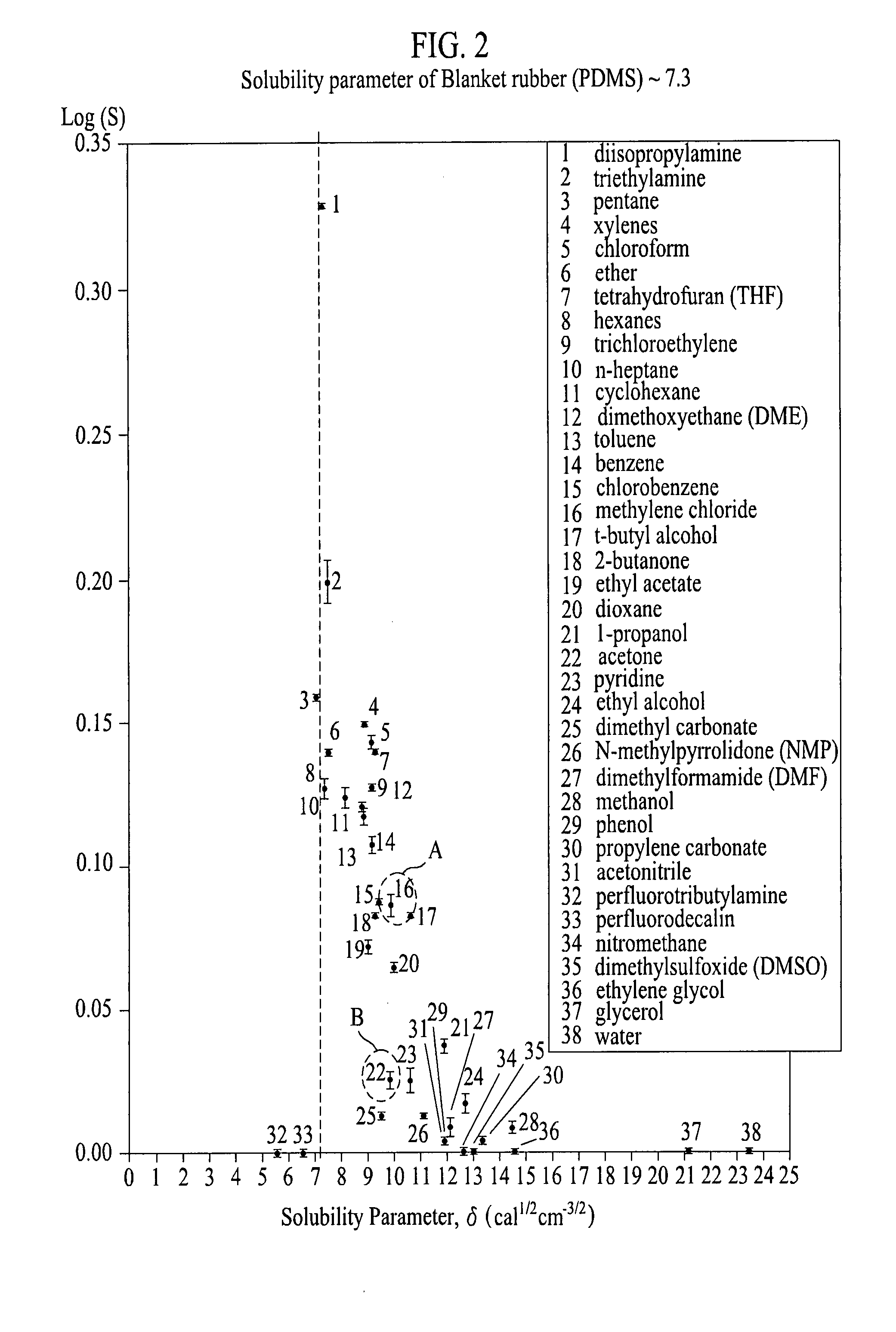
[0035]A material for the solvent in the etch resist solution that does not permeate into the blanket is used in the present invention.

[0036]FIG. 2 shows a graph in which a horizontal axis represents solubility parameter δ of solvents and a vertical axis represents a swelling ratio of PDMS. The solubility parameter δ of PDMS is about 7.3 (cal1 / 2c...


PUM

PropertyMeasurementUnit
Surface tensionaaaaaaaaaa
Viscosityaaaaaaaaaa
Electrical conductoraaaaaaaaaa

Abstract

A method of fabricating a thin film pattern improve the life of a blanket and reduce the cost and improve reliability in forming the thin film pattern. The method includes injecting an etch resist solution into a blanket on a printing roller, wherein the etch resist solution includes a printing solvent that satisfies the condition 6>δsolvent or δsolvent>11, where δsolvent is the solubility parameter of the solvent, or satisfies the condition 6<δsolvent<11 and μ<2(D), where μ is the dipole moment of the solvent; rotating the printing roller to uniformly coat the etch resist solution on the blanket; rolling the printing roller coated with the etch resist solution onto a printing plate to pattern the etch resist solution to thereby form an etch resist pattern; transferring the etch resist pattern from the printing roller to a substrate; hardening the etch resist pattern; and forming a desired thin film pattern on the substrate using the etch resist pattern.

Description

[0001]This application claims the benefit of Korean Patent Application No. 10-2006-0121740, filed on Dec. 4, 2006, which is hereby incorporated by reference for all purposes as if fully set forth herein.BACKGROUND OF THE INVENTION[0002]1. Field of the Invention[0003]The present invention relates to an etch resist solution and a method of fabricating a thin film pattern for a display panel using the etch resist solution. More particularly, the present invention relates to improving the life of a blanket to reduce the cost and improve reliability in forming the thin film pattern.[0004]2. Discussion of the Related Art[0005]Flat panel display devices are popular because they are smaller and lighter than cathode ray tube devices. Examples of flat panel display devices include liquid crystal display devices, field emission display devices, plasma display panel devices and electroluminescence (EL) displays.[0006]In a liquid crystal display device, a picture image is displayed by controllin...

Claims


Application Information

Patent Timeline
IPC IPC(8): C30B33/10
CPCB82Y10/00H01L27/1292G03F7/0002B82Y40/00B41M5/00G02F1/13
Inventor KIM, JIN WUK
Owner LG DISPLAY CO LTD
Why Eureka
Try Eureka