Transformers and baluns

a technology of transformers and baluns, which is applied in the direction of transformer/inductance details, semiconductor devices, semiconductor/solid-state device details, etc., can solve the problems of reducing the scale of transformers, transformers with high inductance, and not yet developed, and achieve high electromagnetic inductance, good symmetry and high magnetic coupling ratio. , the effect of high inductan

Inactive Publication Date: 2008-07-24
SAMSUNG ELECTRONICS CO LTD
View PDF10 Cites 95 Cited by
  • Summary
  • Abstract
  • Description
  • Claims
  • Application Information

AI Technical Summary

Benefits of technology

[0018]According to still yet another aspect of the present invention, at least one each of the primary and secondary coils of the transformer/balun includes an upper coil part extending along the upper surface of one of the insulation layers, a lower coil part, and a plug extending through the insulation layer and into contact with the primary upper and lower coil parts. Thus, such coils can provice a relatively high electromagnetic inductance.
[0019]A transformer or a balun according to the present invention has good symmetry. Additionally, the transformer or the balun may have high inductance by providi...

Problems solved by technology

However, reducing the scale of the transformer compromises its characteristics such as inductance, a magnetic coupling ratio, etc.
However, a compact transformer having high inductance, good symmetry and a high...

Method used


Image

  • Transformers and baluns
  • Transformers and baluns
  • Transformers and baluns

Examples


first embodiment

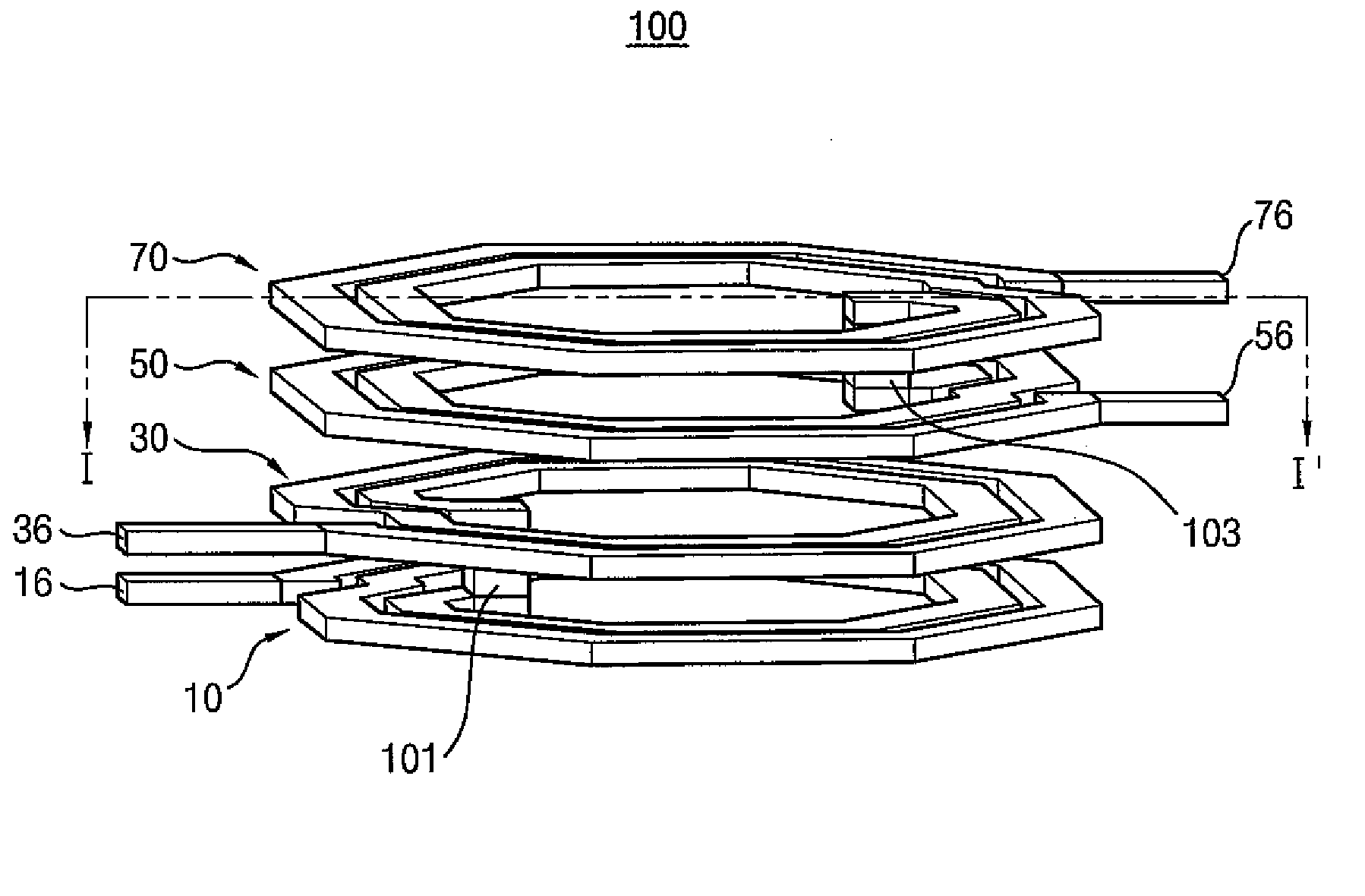
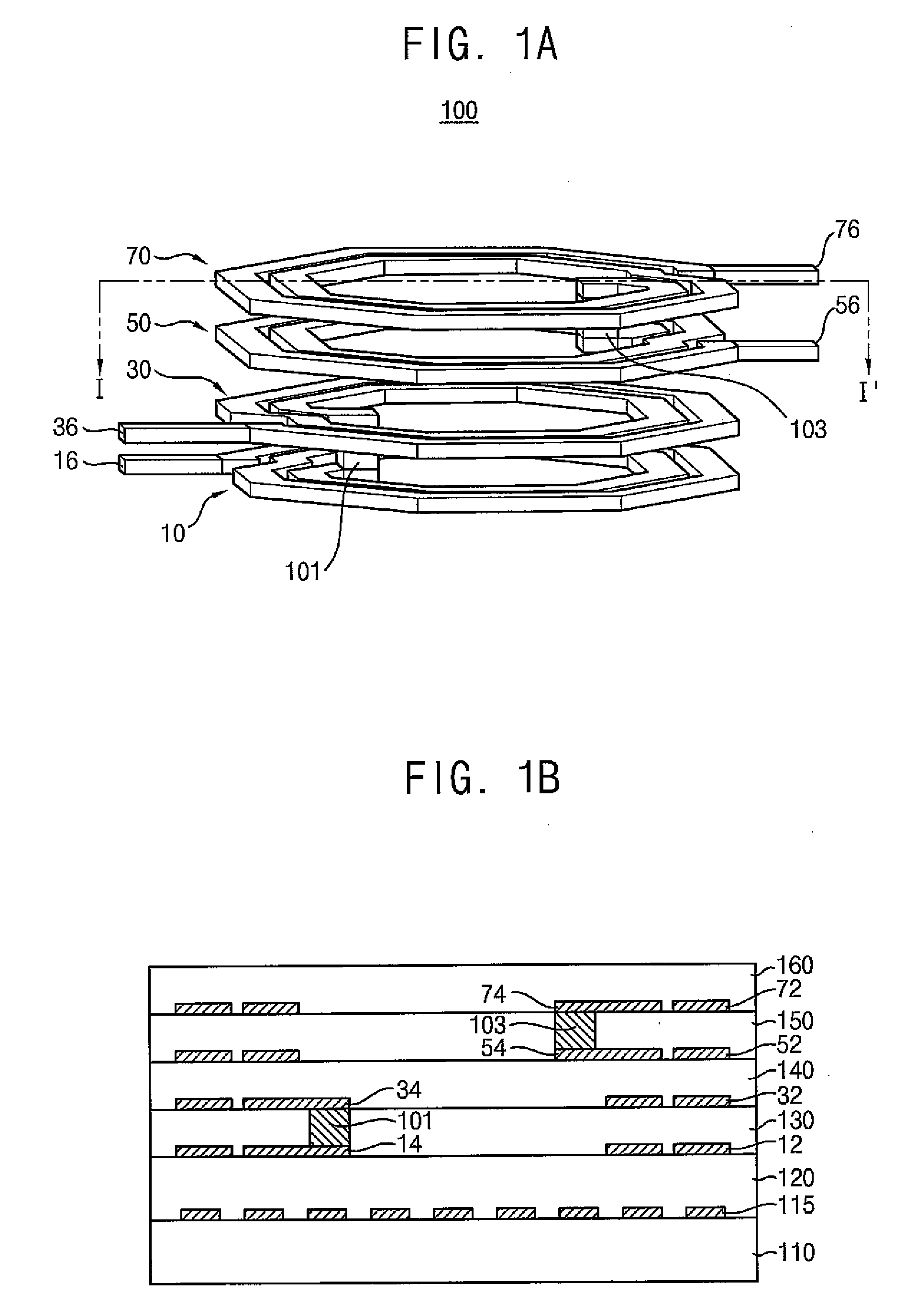
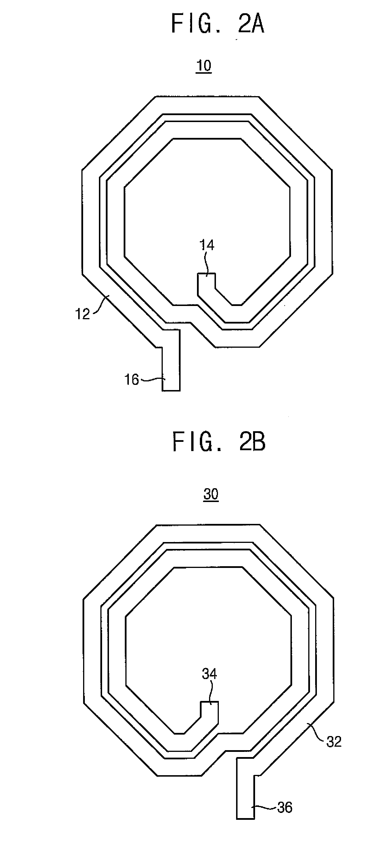
[0040]a transformer 100 in accordance with the present invention will now be described with reference to FIGS. 1A to 1B and 2A to 2D. Note, for clarity a semiconductor substrate and insulation layers of the transformer are not shown in FIG. 1A. The transformer 100 includes a first primary coil 10, a second primary coil 30, a first secondary coil 50, a second secondary coil 70, a primary via 101, and a secondary via 103. The first and second primary coils 10 and 30 together with the primary via 101 constitute a primary coil assembly, and the first and second secondary coils 50 and 70 together with the secondary via 103 constitute a secondary coil assembly. The primary via 101 and the secondary via 103 constitute a first via unit.

[0041]The first and second primary coils 10 and 30 and the first and second secondary coils 50 and 70 are each generally planar and are formed on (extend along) first, second, third and fourth insulation layers 120, 130, 140 and 150, respectively so as to be ...

second embodiment

[0059]a transformer 200 in accordance with the present invention will now be described with reference to FIGS. 3A to 3B and 4A to 4D. The transformer 200 includes a first primary coil 10, a second primary coil 30, a first secondary coil 50, a second secondary coil 70, a primary via 201, and a secondary via 203. The first and second primary coils 10 and 30 together with the primary via 201 constitute a primary coil assembly, and the first and second secondary coils 50 and 70 together with the secondary via 203 constitute a secondary coil assembly. The primary via 201 and the secondary via 203 constitute a second via unit.

[0060]The first primary coil 10, the first secondary coil 50, the second primary coil 30 and second secondary coil 70 are formed on first, second, third and fourth insulation layers 220, 230, 240 and 250, respectively. The insulation layers 220, 230, 240 and 250 are disposed on a substrate 210. The substrate 210 may be of a type which is used in semiconductor devices...

third embodiment

[0064]a transformer 300 in accordance with the present invention will now be described with reference to FIGS. 5 and 6A to 6H. The transformer 300 includes a first primary coil 10, a second primary coil 30, a third primary coil 20, a fourth primary coil 40, a first secondary coil 50, a second secondary coil 70, a third secondary coil 60, a fourth secondary coil 80, a first primary via 301, a second primary via 303, a third primary via 305, a first secondary via 307, a second secondary via 309 and a third secondary via 311. The first to fourth primary coils 10, 30, 20 and 40 together with the first to third primary vias 301, 303 and 305 constitute a primary coil assembly, and the first to fourth secondary coils 50, 70, 60 and 80 together with the first to third secondary vias 307, 309 and 311 constitute a secondary coil assembly. The first to third primary vias 301, 303 and 305 together with the first to third secondary vias 307, 309 and 311 constitute a via unit.

[0065]The coils 10, ...


PUM


Abstract

A transformer includes a primary coil assembly and a secondary coil assembly juxtaposed in a stack and which are electromagnetically inductively coupled and substantially symmetrical to one another. The primary coil assembly includes a plurality of primary coils coplanar with first insulation layers, respectively, and symmetrical to each other, and a first via unit connecting adjacent ones of the primary coils to each other. The secondary coil assembly includes a plurality of secondary coils coplanar with a plurality of second insulation layers, respectively, and symmetrical to each other, and a second via unit connecting adjacent ones of the secondary coils to each other.

Description

BACKGROUND OF THE INVENTION[0001]1. Field of the Invention[0002]The present invention relates to transformers and baluns. More particularly, the present invention relate to a transformer and to a balun that are employed in a system-on-chip (SOC).[0003]2. Description of the Related Art[0004]A system-on-chip (SOC) is an integrated circuit (IC) formed on a single chip. Previously, ICs were typically formed on boards and thereby formed what is commonly known as printed circuit boards (PCBs). An SOC, though, is much more compact than a PCB and may be readily assembled with other electronics. In general, semiconductor elements and radio-frequency (RF) circuit elements are formed on a single chip in an SOC, and an inductor or a transformer is formed on a semiconductor wiring which has already been formed on a substrate of the SOC. The transformer is confined to a small area so that the chip may have a high density, i.e., may be highly integrated. However, reducing the scale of the transfor...

Claims


Application Information

Patent Timeline
IPC IPC(8): H01F27/28
CPCH01F27/2804H01L23/5227H01F2027/2809H01L2924/0002H01L2924/00H01F27/24H01F27/28
Inventor CHOI, TAE-HOONCHUNG, CHUL-HO
Owner SAMSUNG ELECTRONICS CO LTD
Why Eureka
Try Eureka