Depletion-mode mosfet circuit and applications

a mosfet and depletion-mode technology, applied in the field of metal oxide semiconductor field effect transistor simulation and use, can solve the problems of pin assignment error or bug, and the simple way of treating a depletion-type mosfet as a gate-bias shifted enhancement type mosfet has a disadvantage,

Active Publication Date: 2008-07-24
LIN WEN T
View PDF3 Cites 28 Cited by
  • Summary
  • Abstract
  • Description
  • Claims
  • Application Information

AI Technical Summary

Problems solved by technology

This simplistic way of treating a depletion type MOSFET as a gate-bias shifted enhancement type MOSFET has a disadvantage.
Unfortunately, this simplistic treatment of depletion MOSFETs appears to have been built into the Simulation Program with IC Emphasis (SPICE).
Attempts to model depletion-mode MOSFET logic circuits in SPICE apparently result in what appears to be a pin assignment error or bug.

Method used


Image

  • Depletion-mode mosfet circuit and applications
  • Depletion-mode mosfet circuit and applications
  • Depletion-mode mosfet circuit and applications

Examples


Embodiment Construction

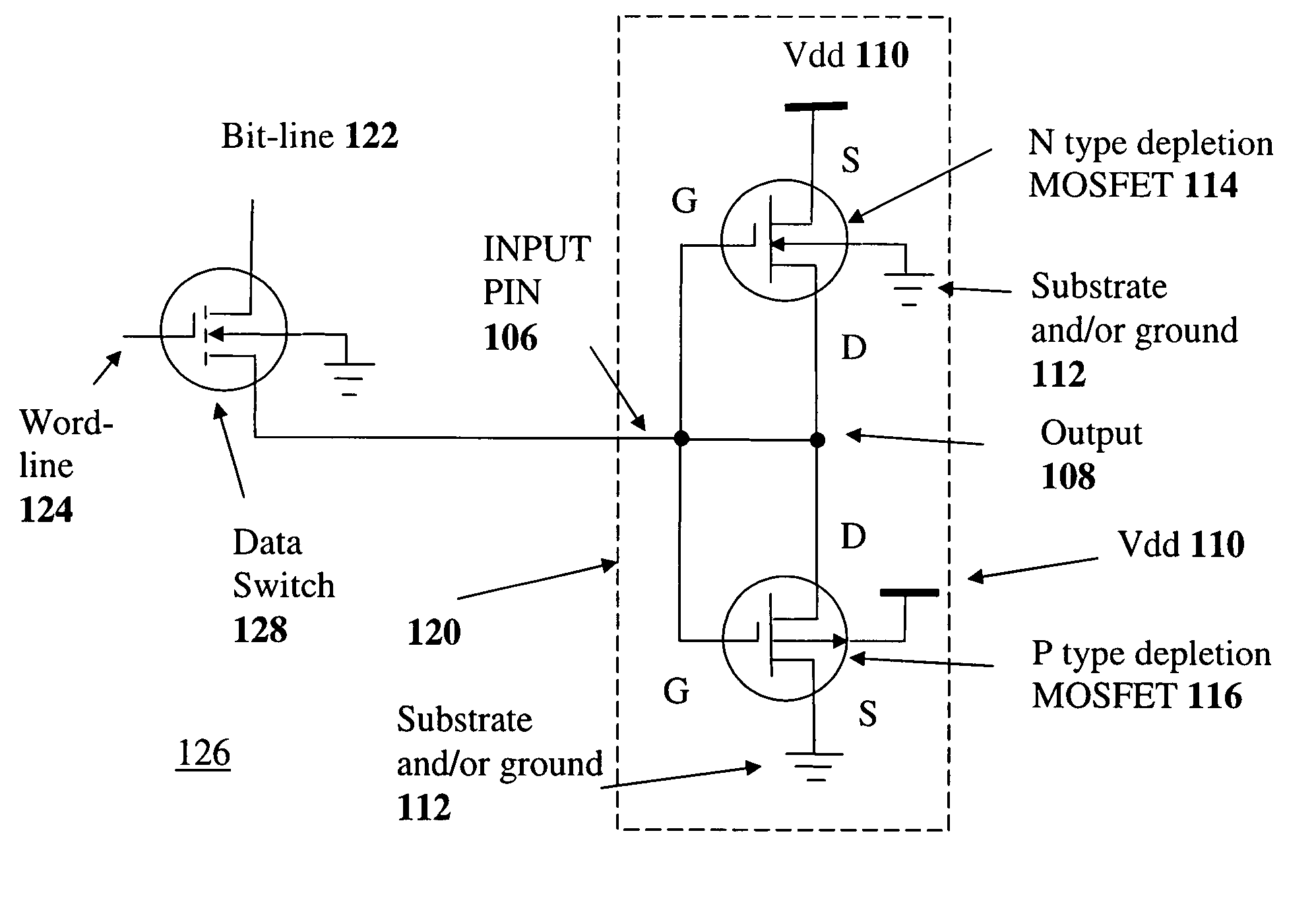
[0059]There is a fundamental difficulty with the computer simulation technology for MOSFET regarding the definition of the source and drain pins; due to the symmetric structure of MOSFET, these two pins are inter-changeable in practice and the definition for the name of source and drain is only nomenclature and immaterial. However, these two pins must be defined precisely in the computer simulation program before the calculations begin. Traditionally, there are two methods to define the pins of MOSFET by using either the DC voltage or majority current carrier. With the voltage method, the pin with lower DC voltage is usually treated as the source and the pin with higher DC voltage is treated as the drain. The other traditional method to identify the source and drain is to use the concept of majority current carrier that whichever pin supplies the majority current carrier is regarded as the source. These two methods, unfortunately, are both imperfect.

[0060]Taking the traditional inve...


PUM


Abstract

Positive logic circuits, systems and methods using MOSFETs operated in a depletion-mode, including electrostatic discharge protection circuits (ESD), non-inverting latches and buffers, and one-to-three transistor static random access memory cells. These novel circuits supplement enhancement-mode MOSFET technology and are also intended to improve the reliability of the complementary metal-oxide-semiconductor (CMOS) integrated circuit (IC) products.

Description

CROSS REFERENCE TO RELATED APPLICATIONS[0001]This application is related to, and claims priority from, U.S. Provisional Patent application No. U.S. 60 / 886,363 filed on Jan. 24, 2007 by W. Lin entitled “Electrostatic Discharge Protection and Prevention for Integrated Circuits”, U.S. Provisional Patent application No. U.S. 60 / 889,614 filed on Feb. 13, 2007 by W. Lin entitled “Logic Circuits using Depletion Type MOSFET Transistors”, U.S. Provisional Patent application No. U.S. 60 / 891,053 filed on Feb. 22, 2007 by W. Lin entitled “Logic Circuits using Depletion Type MOSFET Transistors”, U.S. Provisional Patent application No. U.S. 60 / 894,337 filed on Mar. 12, 2007 by W. Lin entitled “Logic Circuits using Depletion Type MOSFET Transistors” and U.S. Provisional Patent application No. U.S. 60 / 980,506 filed on Oct. 17, 2007 by W. Lin entitled “Depletion MOSFET and its applications”, the contents of all of which are hereby incorporated by reference in their entirety.FIELD OF THE INVENTION[00...

Claims


Application Information

Patent Timeline
Patent Type & Authority Applications(United States)
IPC IPC(8): G11C11/40H03K19/0944H02H9/04
CPCG11C7/1051G11C7/1057G11C7/1078G11C7/1084G11C11/413H01L27/0266H03K3/012H01L2924/0002H03K3/35625H03K19/00323H03K19/09487H01L2924/00
Inventor LIN, WEN T.
Owner LIN WEN T
Why Eureka
Try Eureka