Optical Device and Manufacturing Method of Optical Device

a manufacturing method and optical device technology, applied in the direction of discharge tube/lamp details, instruments, semiconductor lasers, etc., can solve the problems of obstructing the light passage, difficult to provide an adequate optical window aperture, and possible destruction of optical devices, etc., to achieve high reliability, simple and highly productive manufacturing methods, and excellent light input or output characteristics

Active Publication Date: 2008-07-31
ASAHI KASEI ELECTRONICS CO LTD
View PDF4 Cites 66 Cited by
  • Summary
  • Abstract
  • Description
  • Claims
  • Application Information

AI Technical Summary

Benefits of technology

[0032]According to the present invention, an optical device that is highly reliable and is excellent in light input or output characteristic as compared to conventional ones can be obtained. Additionally, a simple and highly productive manufacturing method thereof can be provided. The optical device and manufacturing method thereof of the present invention become an

Problems solved by technology

However, in a case where a optical window is formed by designing a mold such that the a window can be formed, and by performing a sealing step with the mold, it has been difficult to provide an adequate optical window aperture.
This is because burrs of sealing resin inevitably remain on the optical window after the sealing step is performed, obstructing the light passage.
For example, in the case of attempting to perform etching so as to open a hole in the sealing material by a sandblasting method, the optical device may also possibly be destroyed.
Here, if a method disclosed in Patent Document 1 is used, since the elastic body is pressed in the sealing step on the element which detects light, and the element may possibly be broken.
For this reason, there has been a problem where reliability of manufacturing steps becomes low.
Because burrs of the sealing material enter the optical window from a periphery thereof toward a central element thereof in the sealing step, especially, darkening due to burrs is a serious problem in a case where the optical window needs to transmit light with a high transmittance.
Furthermore, in a case where the optical window is provided with a function of adjusting the intensities of light input and output, it is impossible to use the step of removing burrs because the optical device could be destroyed.
This results in a problem of extremely low productivity.
This is because there is no resin material that efficiently transmits the infrared light having long wavelengths, and thus because an epoxy resin package used for an infrared sensor which detects infrared light of not more than about 1 micron, cannot b

Method used


Image

  • Optical Device and Manufacturing Method of Optical Device
  • Optical Device and Manufacturing Method of Optical Device
  • Optical Device and Manufacturing Method of Optical Device

Examples


Embodiment Construction

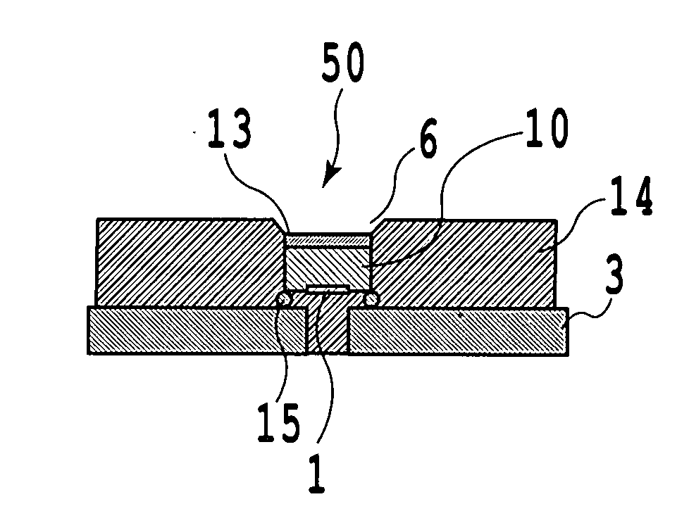
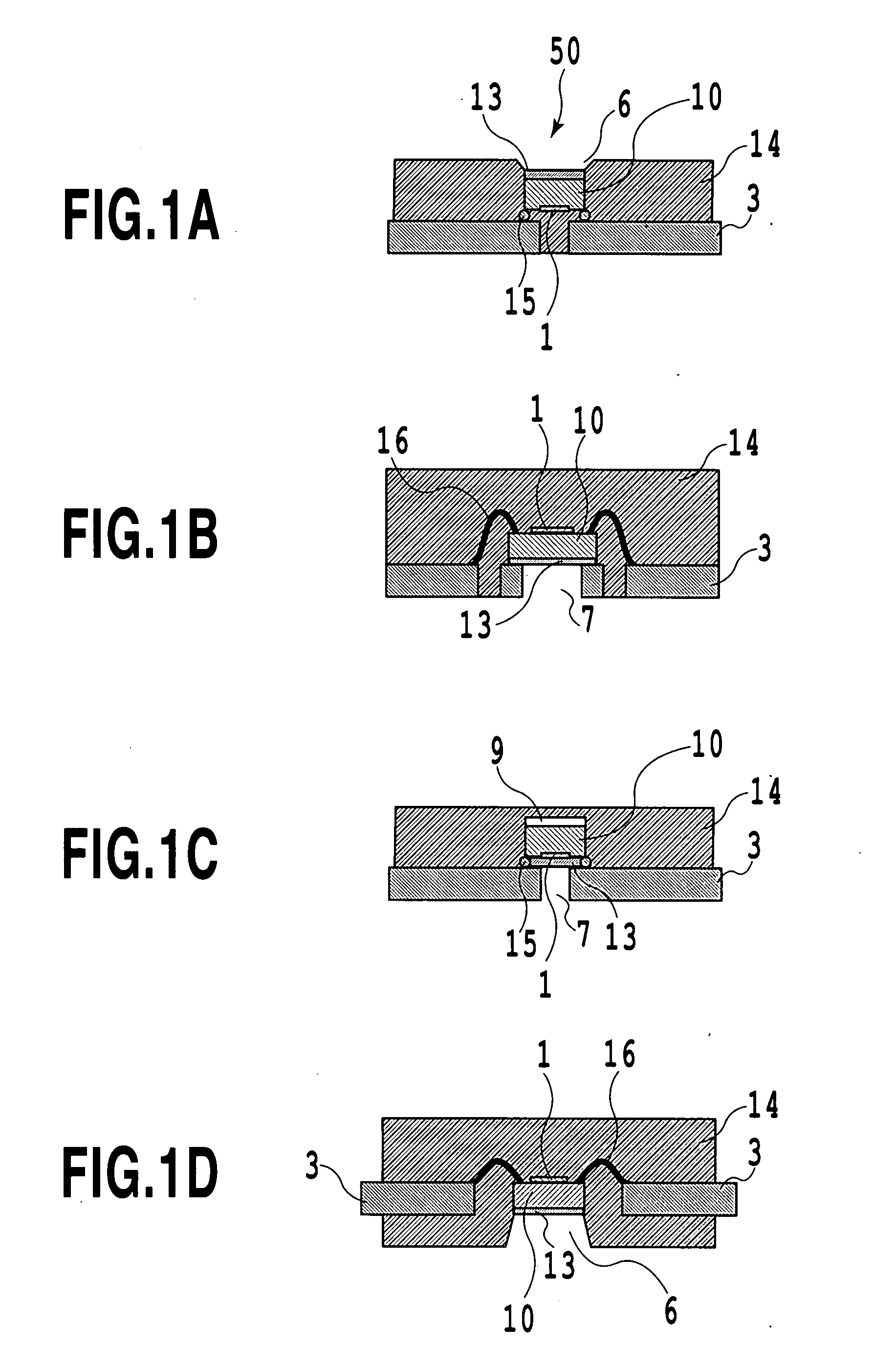
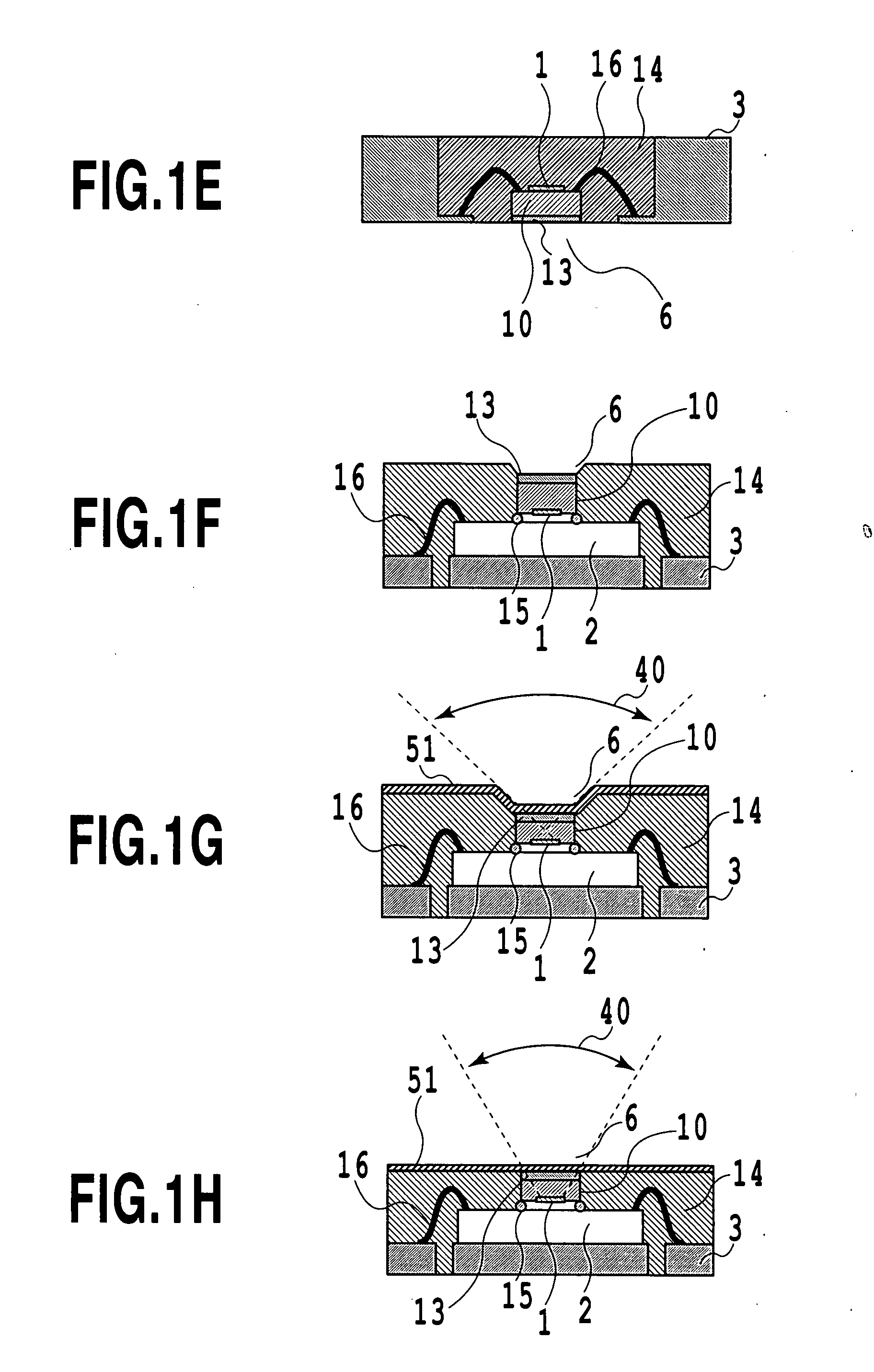
[0078]Embodiments of the present invention will be described in detail below with reference to the drawings. Note that, in the drawings described below, the same reference numerals are given to elements having the same functions, and that,repetitive description thereof will be omitted.

[0079]The present invention proposes an optical device which requires a optical window for allowing light to enter or exit (introducing or deriving light), and can be sealed with resin. That is, in the present invention, elements (a photoelectric conversion element such as a light emitting element or a light receiving element, or a signal transfer element such as a signal processing circuit, and the like) sealed by the sealing material come to be exposed while forming an interface with the outside, and a region thus exposed becomes a optical window for the light path. In the present invention, the elements sealed by the sealing material at least include a photoelectric conversion element, and can inclu...


PUM

PropertyMeasurementUnit
Temperatureaaaaaaaaaa
Thicknessaaaaaaaaaa
Efficiencyaaaaaaaaaa

Abstract

The present invention provides an optical device that is miniature, is highly sensitive and has a simplified package, and a manufacturing method thereof with high production efficiency and high reliability. The present invention is an optical device comprising: a photoelectric conversion element (50) having at least one photoelectric conversion portion (1) which is formed on a substrate (10); a sealing material (14); and a connection terminal (3). The optical device comprises an optical window which is an interface between the photoelectric conversion element (50) and an outside of the optical device; and an aperture (6) formed in the sealing material 14, and whose bottom face is the optical window. An entire face of the optical window is exposed to the outside. An optical adjustment element (13) may be formed on the interface. In this case, the interface between the optical adjustment element (13) and the outside is the optical window.

Description

TECHNICAL FIELD[0001]The present invention mainly relates to a passive or active optical device and a method of manufacturing the optical device.BACKGROUND ART[0002]In each of general electronic devices and optical devices, a sealing material of some kind is required in order to protect a semiconductor chip, which becomes the core of the device, and wiring. In a light emitting element which outwardly outputs an optical signal, or in an optical sensor which detects external light, particularly, the sealing material not only protects the semiconductor chip but also has an important role of fixing in some form a lens and an optical window which are used for derivation or introduction of light. In particular, in the case of a highly sensitive optical sensor, which detects a weak signal, the package of the sensor is designed so as to have the function of stabilizing the temperature of the sensing element, or blocking external electromagnetic noises against the sensing element. On the oth...

Claims


Application Information

Patent Timeline
IPC IPC(8): H01J3/14H01S4/00H01L33/44H01L33/48H01L33/54H01L33/56
CPCH01L25/167Y10T29/49002H01L31/0203H01L33/44H01L33/486H01L33/54H01L33/56H01L33/58H01S5/02248H01S5/02296H01S5/0683H01L2224/16245H01L2224/48247H01L2924/1815H01L27/14618H01L2224/97H01L2924/3025H01L2924/18165H01L2224/73265H01L2224/32245H01L24/97H01L2224/48091H01L2924/00014H01L2924/00H01L2224/73207H01L2924/12041H01L2924/12042H01L2924/12043H01L2924/181H01L2924/18161H01S5/02257H01S5/02325H01L2924/00012
Inventor CAMARGO, EDSON GOMESNAGASE, KAZUHIROKURIHARA, MASAAKIKANAYAMA, YUICHI
Owner ASAHI KASEI ELECTRONICS CO LTD
Why Eureka
Try Eureka