Supercharge Your Innovation With Domain-Expert AI Agents!

Passive Processing Device For Interfacing and For Esd and Radio Signal Rejection in Audio Signal Paths of an Electronic Device

a technology of electronic devices and audio signals, applied in the direction of electrical transducers, substation equipment, emergency protective arrangements for limiting excess voltage/current, etc., can solve the problems of affecting the efficiency of pcb layout, affecting the efficiency of mobile phone development, and affecting the quality of mobile phone reception, etc., to achieve the effect of improving the situation

Active Publication Date: 2008-07-31
NXP BV
View PDF11 Cites 0 Cited by
  • Summary
  • Abstract
  • Description
  • Claims
  • Application Information

AI Technical Summary

Benefits of technology

[0009]So, the object of this invention is to improve the situation.

Problems solved by technology

This burst noise is usually demodulated by the baseband processor's inner amplifiers and / or the microphone, which pollutes the audio signals to be transmitted.
Moreover, since the tracks where the components are soldered bring additional resistive (R) and inductance (L) components to their RLC model, new capacitance values must be computed for each capacitor component each time the layout of the mobile phone Printed Circuit Board (PCB) is modified, which is time-consuming and, therefore, expensive for mobile phone development.
This area occupancy prevents efficient layout of the PCB.

Method used


Image

  • Passive Processing Device For Interfacing and For Esd and Radio Signal Rejection in Audio Signal Paths of an Electronic Device
  • Passive Processing Device For Interfacing and For Esd and Radio Signal Rejection in Audio Signal Paths of an Electronic Device
  • Passive Processing Device For Interfacing and For Esd and Radio Signal Rejection in Audio Signal Paths of an Electronic Device

Examples


Embodiment Construction

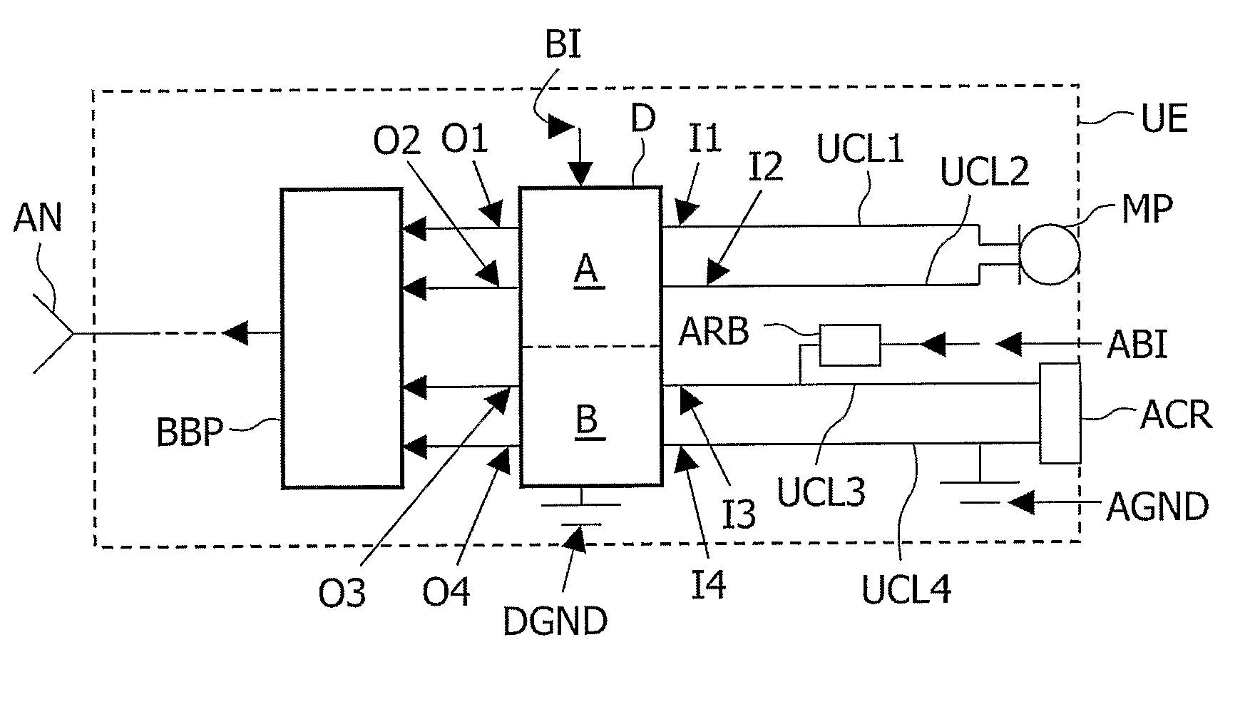
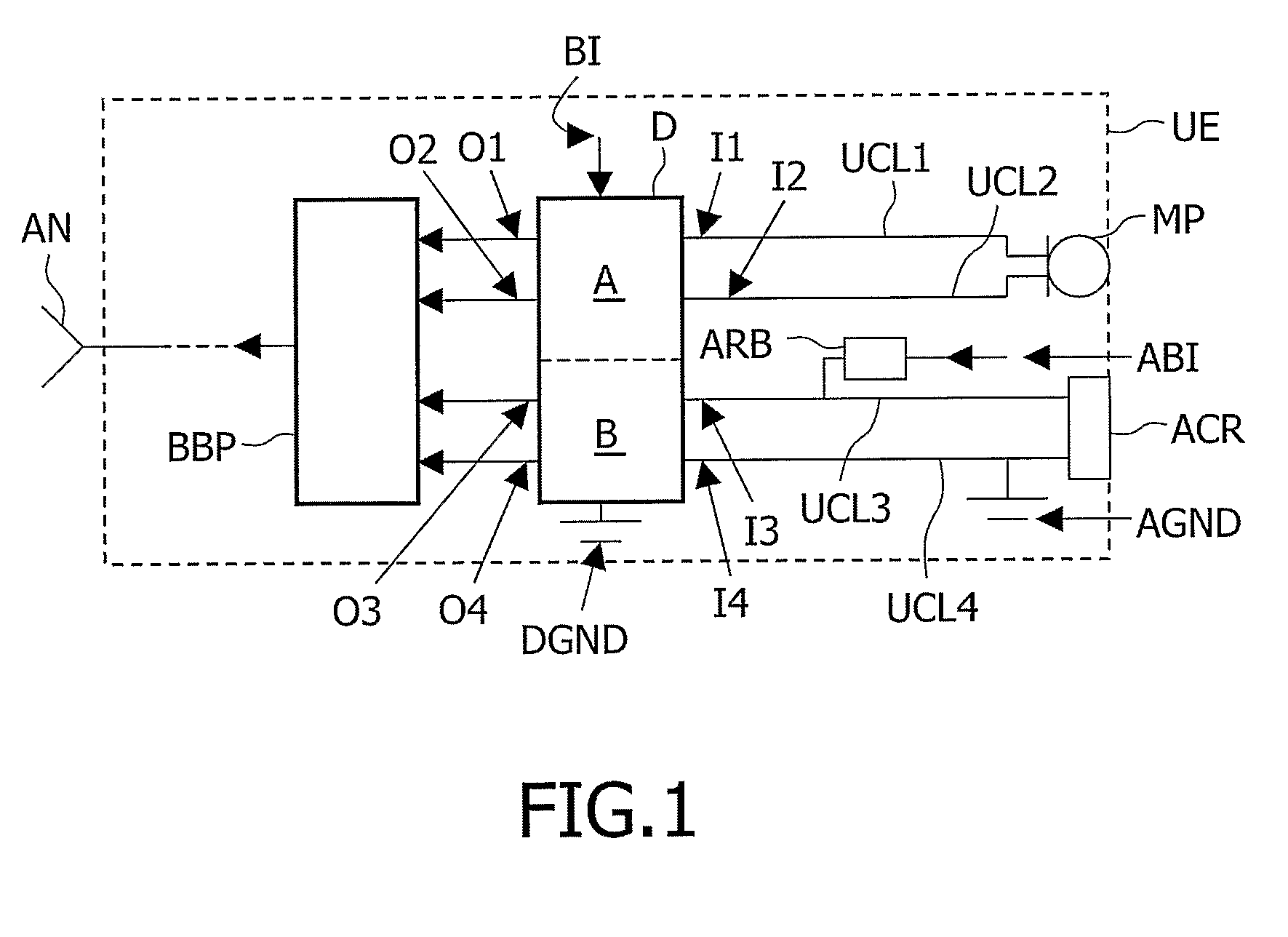
[0031]Reference is initially made to FIG. 1 to describe an example of a mobile communication device UE in which the invention may be applied.

[0032]In the following description it will be considered that the device shown is a mobile phone UE, for instance a GSM / GPRS or UMTS mobile phone. But it is important to notice that the invention is not limited to this type of mobile communication device. Indeed this invention may be applied to any mobile communication device (such as a GSM card embedded in a computer) in which the audio signals picked up by a microphone and / or an audio accessory may be polluted by the radio signals transmitted by the antenna.

[0033]Moreover, the audio signal amplification paths being the only parts of the mobile phone UE to which the invention is applied, only these amplification paths will be focused on in the following description.

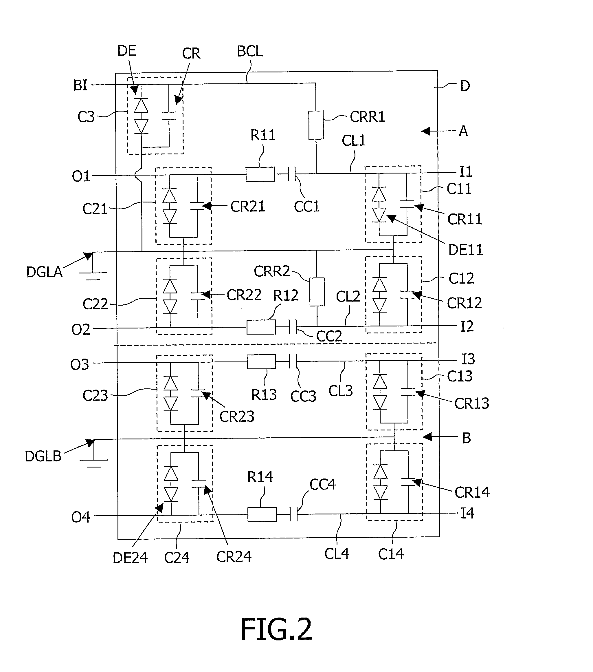
[0034]The illustrated mobile phone UE comprises schematically a microphone MP and an audio connector ACR, each having two outputs ...


PUM


Abstract

A passive processing device (D) is adapted to be interfaced in a full integrated way on at least a first audio signal path defined between a first audio signal source and an audio signal processing means of an electronic device, such as a mobile communication device. This device (D) comprises a first protection means (DE11; DE12) for rejecting electrostatic discharges on the first path, a first rejection means (CR11, R11; CR12) for rejecting radio signals at least in a chosen frequency band on the first path, and a first AC-coupling means (CC1) for interfacing voltage levels between the first audio signal source and the audio signal processing means.

Description

FIELD OF THE INVENTION[0001]The present invention relates to audio signal processing in electronic devices such as mobile communication devices.BACKGROUND OF THE INVENTION[0002]As it is known by one skilled in the art, certain electronicdevices, such as mobile communication devices, and notably mobile phones, have one or more audio signal amplification paths, such as microphone and audio accessory amplification paths that are subjected to a burst noise, which disturbs the audio signals. This burst noise mainly comes from the radio signals that are transmitted by the device antenna through bursts at different frequencies, such as 900 MHz and 1800 MHz (square-wave signal with Tcycle=4.615 ms Cyclic ratio ⅛ modulated by radio signal at a frequency of 900 MHz, for instance). This modulated signal is picked up by the microphone and / or audio accessory, but also by the conductive lines connecting the microphone and / or audio accessory connector to a baseband processor.[0003]This burst noise...

Claims


Application Information

Patent Timeline
IPC IPC(8): H04B15/00H02H9/04
CPCH04B15/00
Inventor LE MELLAT, BERTRAND JEAN-LOUIS
Owner NXP BV
Features
  • R&D
  • Intellectual Property
  • Life Sciences
  • Materials
  • Tech Scout
  • Unparalleled Data Quality
  • Higher Quality Content
  • 60% Fewer Hallucinations
Learn More