Method for production of thin-film semiconductor device

a technology of semiconductor devices and thin films, applied in the direction of semiconductor devices, electrical devices, transistors, etc., can solve the problems of reducing increasing the fixed amount of oxynitride (sion) film, and increasing the vth of tft, so as to reduce the interface state, reduce the fixed charge, and reduce the effect of fixed charg

Inactive Publication Date: 2008-07-31
JAPAN DISPLAY INC
View PDF2 Cites 29 Cited by
  • Summary
  • Abstract
  • Description
  • Claims
  • Application Information

AI Technical Summary

Benefits of technology

[0013]According to an embodiment of the present invention, the method mentioned above includes the fourth step for heat treatment in an oxygen-containing atmosphere, with a semiconductor film covering the gate insulating film. This step causes oxygen in the oxidizing atmosphere to reach the gate insulating film through the semiconductor film, thereby supplying oxygen to oxygen deficient parts in the gate insulating film. This procedure eliminates fixed charges in the gate insulating film of silicon oxynitride and interface states between the semiconductor film and the gate insulating film.
[0014]In addition, the heat treatment mentioned above causes an oxide film to grow as the surface of the semiconductor film is oxidized. The resulting thermal oxi...

Problems solved by technology

As mentioned above, the disadvantage of TFTs of bottom gate type having a silicon oxynitride (SiON) film as the underlying gate insulating film for poly-Si film is that the silicon oxynitride (SiON) film still has more fixed charges and interface states th...

Method used


Image

  • Method for production of thin-film semiconductor device
  • Method for production of thin-film semiconductor device
  • Method for production of thin-film semiconductor device

Examples


first embodiment

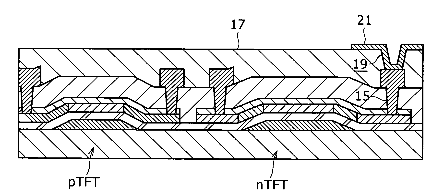
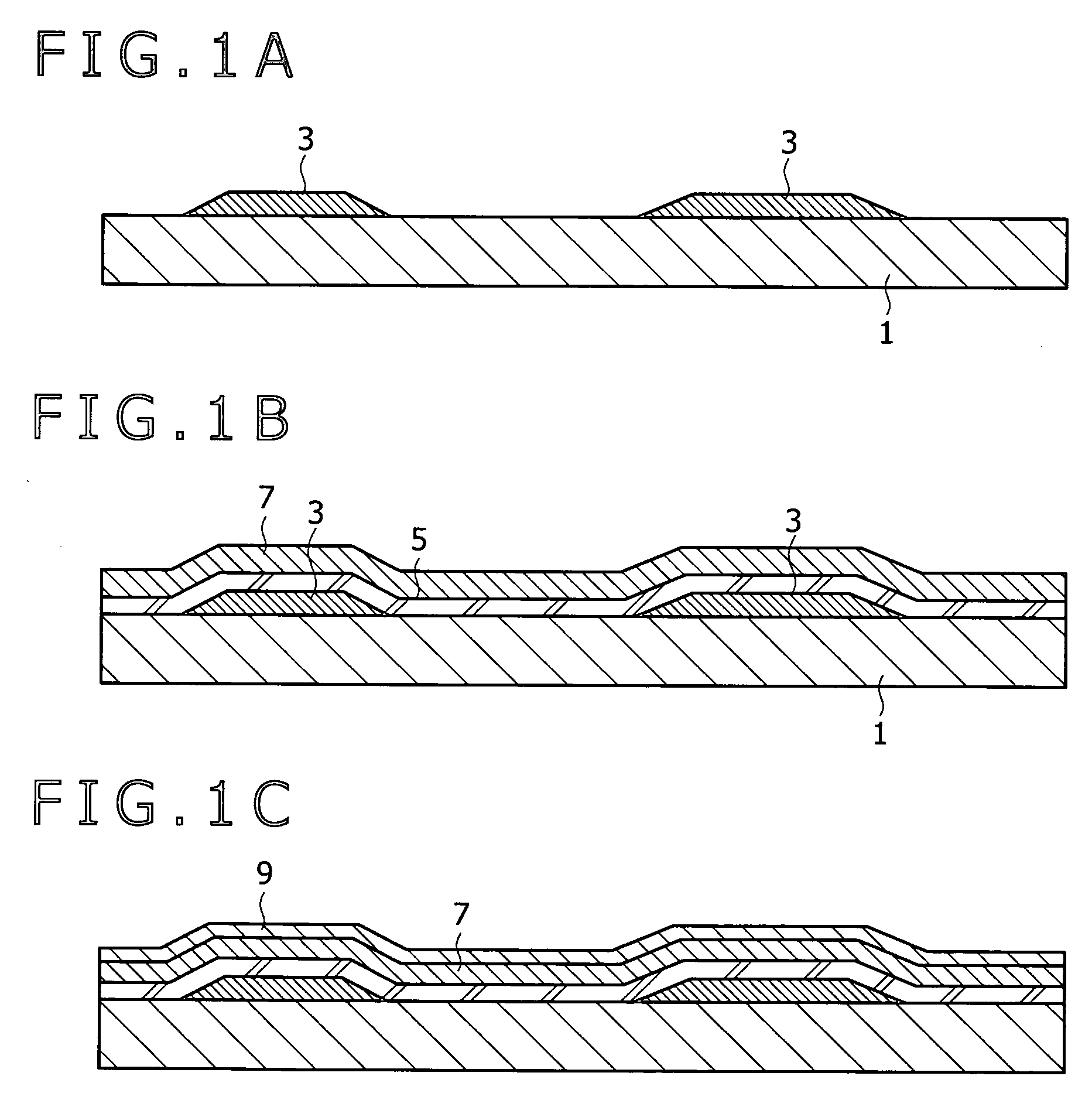
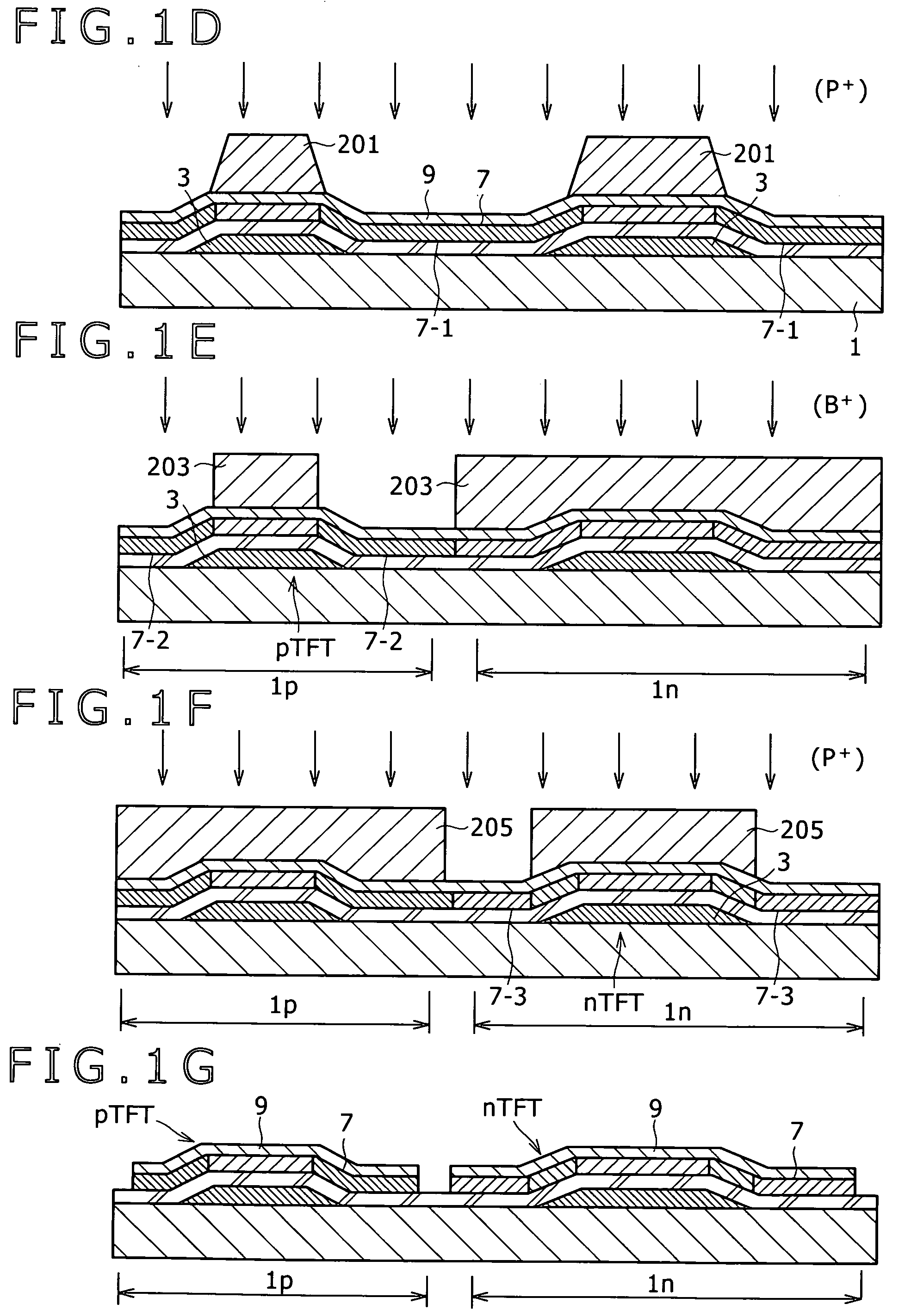
[0025]FIGS. 1A to 1J are sectional views showing steps in the first embodiment of the method for production of a thin-film semiconductor device according to an embodiment of the present invention. The embodiment mentioned below is intended for the drive panel of the display unit provided with TFTs of planar bottom gate type in the form of CMOS.

[0026]The first step shown in FIG. 1A starts with getting ready an insulating substrate 1, which may be “AN100” from Asahi Glass CO. LMT. or “Code 1737” from Corning Incorporated, for example.

[0027]The substrate 1 has gate electrodes 3 formed thereon by patterning. The gate electrodes 3 are formed from film of Mo, W, Ta, or Cu by sputtering and ensuing patterning.

[0028]Incidentally, the thickness of the gate electrode (metal film) should be 30 to 200 nm.

[0029]The next step shown in FIG. 1B is intended to form a gate insulating film of silicon oxynitride (SiOxNy) 5 (which will be referred to as SiON gate insulating film hereinafter) on the gate...

second embodiment

[0056]FIGS. 3A to 3F are sectional views showing steps in the second embodiment of the method for production of a thin-film semiconductor device according to the embodiment of the present invention. The embodiment mentioned below is intended for the drive panel of the display unit provided with bottom gate TFTs of channel stop type with the n-channel only.

[0057]The same procedure as mentioned above for the first embodiment with reference to FIGS. 1A to 1C are repeated to cover the gate electrodes 3 on the insulating substrate 1 sequentially with the SiON gate insulating film 5 and the semiconductor thin film 7 and then perform steam annealing under pressure for modification of the SiON gate insulating film 5 and growth of the thermal oxide film 9 on the surface of the semiconductor thin film 7.

[0058]The next step shown in FIG. 3A is intended to form a resist pattern 207 which overlaps the gate electrode 3 on the thermal oxide film 9 by back surface exposure through the substrate 1, ...

third embodiment

[0069]FIGS. 4A to 4E are sectional views showing steps in the third embodiment of the method for production of a thin-film semiconductor device according to the embodiment of the present invention. The embodiment mentioned below is intended for the drive panel of the display unit provided with dual gate TFTs of CMOS type.

[0070]The same procedure as mentioned above for the first embodiment with reference to FIGS. 1A to 1C are repeated to cover the gate electrodes 3 on the insulating substrate 1 sequentially with the SiON gate insulating film 5 and the semiconductor thin film 7 and then perform steam annealing under pressure for modification of the SiON gate insulating film 5 and growth of the thermal oxide film 9 on the surface of the semiconductor thin film 7. The foregoing steps are followed by the same procedure as described above with reference to FIGS. 1D to 1G, by which both the thermal oxide film 9 and the semiconductor thin film 7 undergo pattern etching so that they are divi...


PUM


Abstract

Disclosed herein is a method for production of a thin-film semiconductor device which includes, a first step to form a gate electrode on a substrate, a second step to form a gate insulating film of silicon oxynitride on the substrate in such a way as to cover the gate electrode, a third step to form a semiconductor thin film on the gate insulating film, and a fourth step to perform heat treatment in an oxygen-containing oxidizing atmosphere for modification through oxygen binding with oxygen-deficient parts in the silicon oxynitride film constituting the gate insulating film.

Description

CROSS REFERENCES TO RELATED APPLICATIONS[0001]The present invention contains subject matter related to Japanese Patent Application JP 2007-020614 filed in the Japan Patent Office on Jan. 31, 2007, the entire contents of which being incorporated herein by reference.BACKGROUND OF THE INVENTION[0002]1. Field of the Invention[0003]The present invention relates to a method for production of a thin-film semiconductor device and, more particularly, to a method for production of a thin-film semiconductor device of bottom gate type.[0004]2. Description of the Related Art[0005]Flat panel displays, such as liquid crystal displays and organic EL displays, have thin-film transistors (TFTS) as elements to drive pixel electrodes. Of these TFTS, poly-Si TFTs in which the semiconductor thin film constituting the active layer is made of poly-Si are attracting attention because they form driving circuits and permit highly functional circuits to be built into the panel thereby giving the so-called syst...

Claims


Application Information

Patent Timeline
IPC IPC(8): H01L21/336H01L21/8238H01L27/08H01L27/092H01L29/786
CPCH01L27/1214H01L29/78648H01L29/4908H01L27/1259H01L21/02126H01L21/02249H01L21/324
Inventor KUNII, MASAFUMI
Owner JAPAN DISPLAY INC
Why Eureka
Try Eureka