Asymmetric MIM Capacitor for DRAM Devices

a technology of dram capacitor and mim, which is applied in the direction of capacitors, semiconductor devices, electrical apparatus, etc., can solve the problems of difficult use of crystalline moosub>2 as a second electrode in mim dram capacitor, undesirable high temperature processes in the manufacture of dram devices, and degrade the performance of moosub>2 and other problems, to achieve the effect of increasing the conductivity of the layer and reducing the interface sta

Inactive Publication Date: 2013-04-18
INTERMOLECULAR
View PDF3 Cites 1 Cited by
  • Summary
  • Abstract
  • Description
  • Claims
  • Application Information

AI Technical Summary

Benefits of technology

[0017]In some embodiments of the present invention, a thin layer of SnO2 or RuO2 is formed on top of the dielectric material. The capacitor stack may then be subjected to a PMA treatment in an oxidizing atmosphere to fill the oxygen vacancies in the dielectric material and reduce the interface states at the dielectric / second electrode interface. A thicker, high conductivity layer may then be formed on top of the thin layer to complete the formation of the second electrode. An additional PMA treatment is not required after the formation of the thick layer. The thin layer of SnO2 or RuO2 may be doped to further increase the layer's conductivity.

Problems solved by technology

However, high temperature processes are undesirable in the manufacture of DRAM devices.
However, oxygen-rich phases (MoO2+x) degrade the performance of the MoO2 electrode because they do not promote the deposition of the rutile-phase of TiO2 and have higher resistivity than MoO2.
The use of crystalline MoO2 as a second electrode in MIM DRAM capacitors has been difficult due to a number of problems.
As discussed above, MoO2 is sensitive to oxidation to form oxygen-rich compounds that negatively impacts its performance as an electrode material.
The reducing atmosphere anneal processes discussed previously with respect to the use of crystalline MoO2 as a first electrode are not an option at this stage of the device manufacture because they would degrade the performance of the dielectric layer through the formation of oxygen vacancies.
TiO2 high k dielectric materials are especially sensitive to processing conditions and increases in the leakage current are observed, likely due to the formation of oxygen vacancies.
The asymmetric stack provides a number of problems.
First, Ru is expensive and increases the cost of manufacturing for the DRAM device.
Second, the leakage current of the MIM DRAM device increases at high temperatures (i.e. 90 C) to above the desired target of −7 A cm−2 at 1V.
Third, if a PMA treatment in a dilute oxidizing atmosphere is required after the formation of the second electrode, the control of the Ru second electrode layer is difficult.
Additionally, the formation of RuO2 induces an unacceptably high surface roughness.

Method used


Image

  • Asymmetric MIM Capacitor for DRAM Devices
  • Asymmetric MIM Capacitor for DRAM Devices
  • Asymmetric MIM Capacitor for DRAM Devices

Examples


Embodiment Construction

[0024]A detailed description of one or more embodiments is provided below along with accompanying figures. The detailed description is provided in connection with such embodiments, but is not limited to any particular example. The scope is limited only by the claims and numerous alternatives, modifications, and equivalents are encompassed. Numerous specific details are set forth in the following description in order to provide a thorough understanding. These details are provided for the purpose of example and the described techniques may be practiced according to the claims without some or all of these specific details. For the purpose of clarity, technical material that is known in the technical fields related to the embodiments has not been described in detail to avoid unnecessarily obscuring the description.

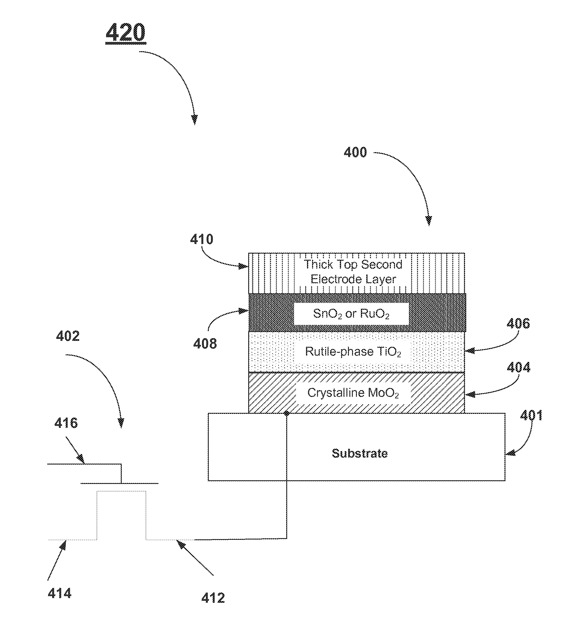
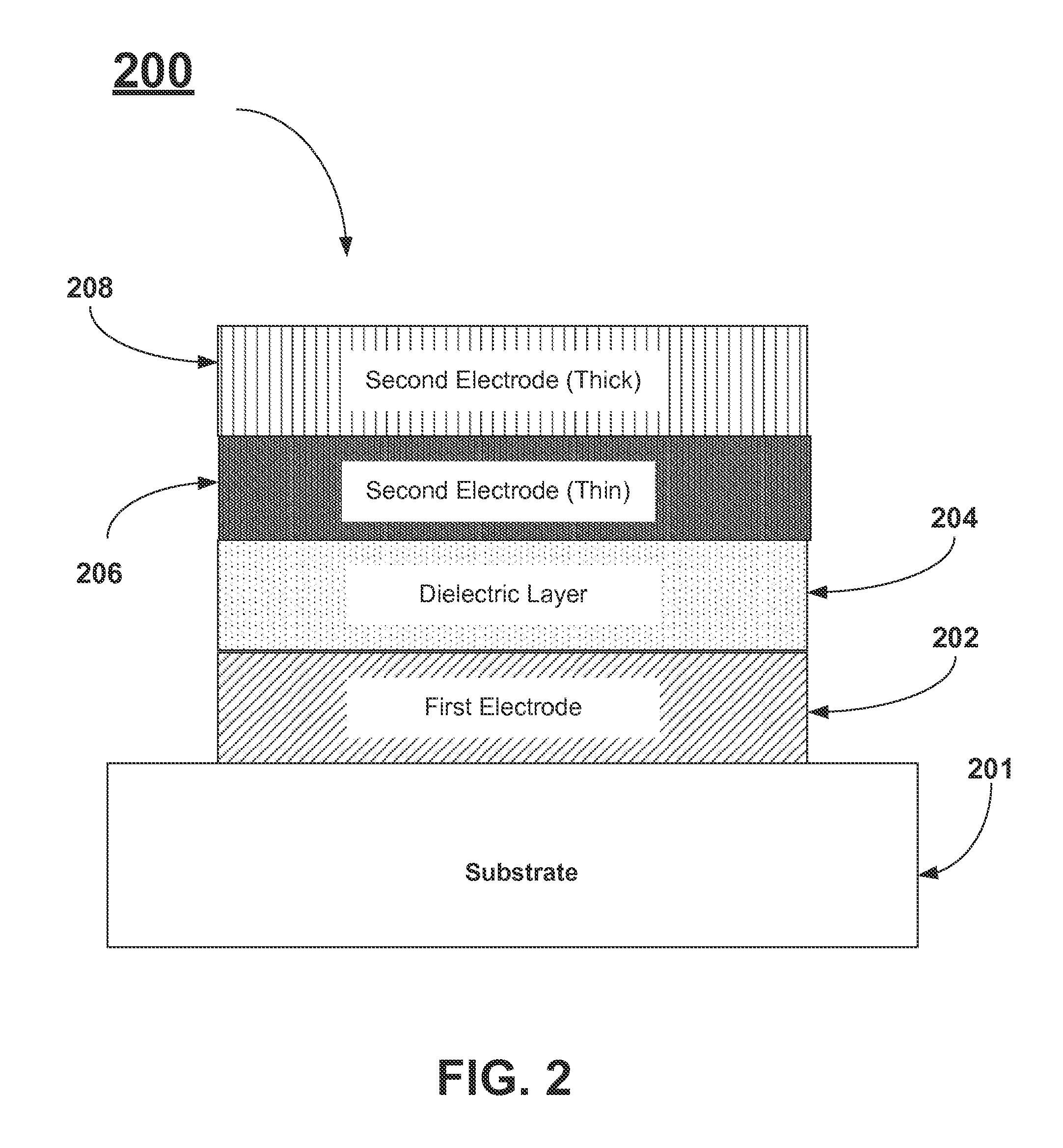
[0025]FIG. 1 describes a method, 100, for fabricating a DRAM capacitor stack. The initial step, 102, comprises forming a first electrode layer on a substrate. Examples of suit...


PUM

PropertyMeasurementUnit
thicknessaaaaaaaaaa
thicknessaaaaaaaaaa
thicknessaaaaaaaaaa

Abstract

A bilayer second electrode for a MIM DRAM capacitor is formed wherein the layer of the electrode that is in contact with the dielectric layer (i.e. bottom layer) has a composition that is resistant to oxidation during subsequent anneal steps and have rutile templating capability. Examples include SnO2 and RuO2. The capacitor stack including the bottom layer is subjected to a PMA treatment to reduce the oxygen vacancies in the dielectric layer and reduce the interface states at the dielectric / second electrode interface. The other component of the bilayer (i.e. top layer) is a high work function, high conductivity metal or conductive metal compound.

Description

CROSS-REFERENCE TO RELATED APPLICATIONS[0001]This is a Continuation Application of U.S. patent application Ser. No. 13 / 195,528 filed on Aug. 1, 2011, which is herein incorporated by reference for all purposes.[0002]This document relates to the subject matter of a joint research agreement between Intermolecular, Inc. and Elpida Memory, Inc.FIELD OF THE INVENTION[0003]The present invention relates generally to the use of non-noble metal electrodes in capacitors used in Dynamic Random Access Memory (DRAM) devices.BACKGROUND OF THE INVENTION[0004]Dynamic Random Access Memory utilizes capacitors to store bits of information within an integrated circuit. A capacitor is formed by placing a dielectric material between two electrodes formed from conductive materials. A capacitor's ability to hold electrical charge (i.e., capacitance) is a function of the surface area of the capacitor plates A, the distance between the capacitor plates d (i.e. the physical thickness of the dielectric layer), ...

Claims


Application Information

Patent Timeline
Patent Type & Authority Applications(United States)
IPC IPC(8): H01L49/02
CPCH01L27/10805H01L28/75H01L28/65H10B12/30
Inventor CHEN, HANHONGODE, HIROYUKI
Owner INTERMOLECULAR
Why Eureka
Try Eureka