Semiconductor device and method of manufacturing the same

a technology of semiconductor devices and semiconductor devices, applied in the direction of semiconductor devices, electrical devices, transistors, etc., can solve the problems of deteriorating the reliability of semiconductor devices, increasing current leakage, and generating current, and achieve the effect of reducing the interface sta

Inactive Publication Date: 2011-05-03
LONGITUDE LICENSING LTD
View PDF6 Cites 5 Cited by
  • Summary
  • Abstract
  • Description
  • Claims
  • Application Information

AI Technical Summary

Benefits of technology

[0017]Accordingly, it is a primary object of the present invention to provide a semiconductor device with reduced interface state.
[0018]It is another object of the present invention to provide a semiconductor device with fluorine-introduced interface to suppress generation of defects and reduce interface state.
[0019]It is a further object of the present invention to provide a semiconductor device with reduced variation of performance.

Problems solved by technology

The interface state may cause generation current and increase leakage of current unless the interface state is sufficiently reduced to suppress such generation current and leakage of current.
The interface state may cause variation of threshold voltage over time and deteriorate the reliability of the semiconductor device.
In a memory cell of a dynamic random access memory (DRAM), increase of leakage of current or variation of threshold voltage may deteriorate refresh performance.
Si—H bonds are likely to be broken by thermal stress application and hot carrier injection, thereby generating dangling bonds.
Direct implantation of fluorine into a silicon substrate may generate a large number of point defects in the silicon substrate.
Such high temperature heat treatment makes it difficult to realize the shrinkage of a semiconductor device.
Low temperature heat treatment that is suitable for realizing the shrinkage of a semiconductor device may cause insufficient recovery, thereby allowing point defects to reside in a depletion layer.
Such residual point defects may cause junction leakage, thereby deteriorating the performance of a semiconductor device.

Method used


Image

  • Semiconductor device and method of manufacturing the same
  • Semiconductor device and method of manufacturing the same
  • Semiconductor device and method of manufacturing the same

Examples


example

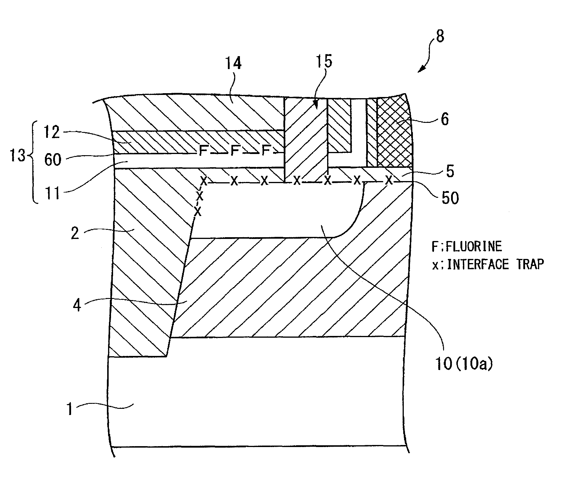
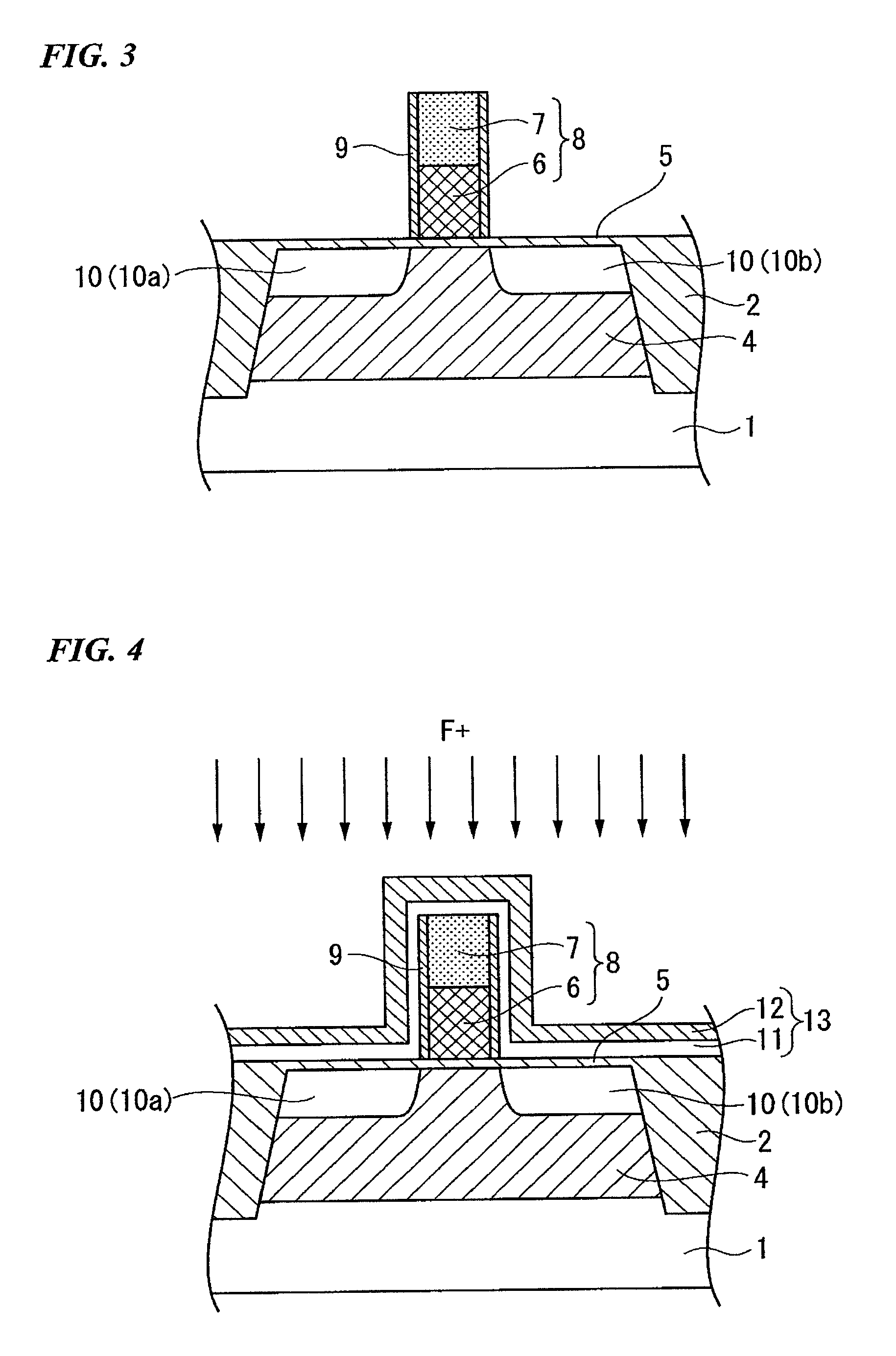
[0129]An n-type MOSFET (Metal Oxide Semiconductor Field Effect Transistor) was prepared in accordance with the processes shown in FIGS. 1-6.

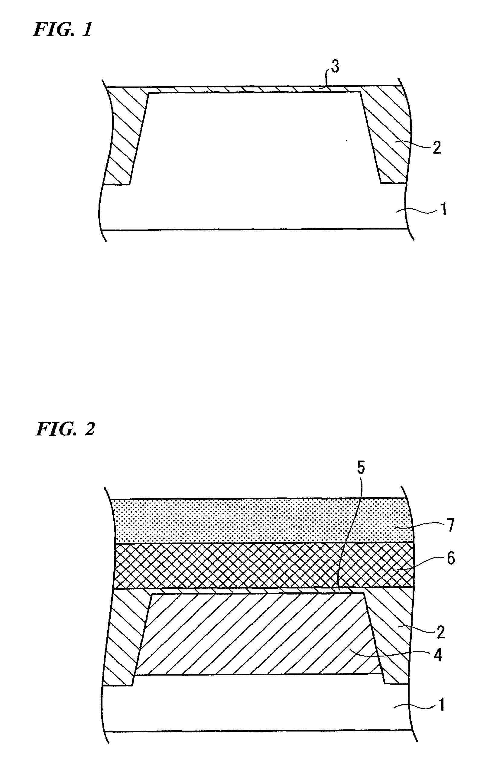
[0130]With reference to FIG. 1, a silicon substrate 1 was prepared. A groove was formed in a shallow portion of the silicon substrate 1, wherein the groove isolates or defines an active region of the silicon substrate 1. A buried insulating film 2 was formed in the groove of the silicon substrate 1 so as to isolate the active region of the silicon substrate 1. A silicon oxide film 3 having a thickness of 10 nanometers was formed on the surface of the silicon substrate 1 by a thermal oxidation process.

[0131]An ion-implantation process was carried out to introduce boron into the active region of the silicon substrate 1 through the silicon oxide film 3, thereby forming a p-type diffusion layer 4 in the active region of the semiconductor substrate 1. The ion-implantation process was carried out under first conditions at acceleration energy of 300 ke...


PUM


Abstract

A semiconductor device may include a semiconductor substrate, a diffusion layer provided over the semiconductor substrate, source and drain diffusion regions provided in upper regions of the diffusion layer, a gate insulating film provided over the source and drain diffusion regions and the diffusion layer, a gate electrode provided on the gate insulating film and positioned over the diffusion layer, a passivation film provided over the gate insulating film and the gate electrode, an insulating film that covers the passivation film, and contact plugs that penetrate the insulating film, the passivation film, and the gate insulating film, so that the contact plugs reach the source and drain diffusion regions. The contact plugs are positioned near side walls of the gate electrode. Fluorine is implanted to the passivation film. Fluorine is diffused to a silicon-insulator interface between the gate insulating film and the diffusion layer under the gate electrode.

Description

BACKGROUND OF THE INVENTION[0001]1. Field of the Invention[0002]The present invention generally relates to a semiconductor device and a method of manufacturing the same. More specifically, the present invention relates to an MOS semiconductor device having an interface between a semiconductor layer and an insulating layer, wherein the interface has a reduced interface state, and the MOS semiconductor device has suppressed variation of performances and reduced leakage of current.[0003]Priority is claimed on Japanese Patent Application No. 2007-102493, filed Apr. 10, 2007, the content of which is incorporated herein by reference.[0004]2. Description of the Related Art[0005]All patents, patent applications, patent publications, scientific articles, and the like, which will hereinafter be cited or identified in the present application, will hereby be incorporated by reference in their entirety in order to describe more fully the state of the art to which the present invention pertains.[...

Claims


Application Information

Patent Timeline
Patent Type & Authority Patents(United States)
IPC IPC(8): H01L29/72
CPCH01L21/26506H01L21/76825H01L29/0847H01L21/76832H01L29/78
Inventor TAKETANI, HIROAKI
Owner LONGITUDE LICENSING LTD
Why Eureka
Try Eureka