Method of manufacturing GaN-based transistors

a technology of field effect transistor and manufacturing method, which is applied in the direction of basic electric elements, electrical apparatus, and semiconductor devices, can solve problems such as the interface state being worsened

Active Publication Date: 2011-05-17
FURUKAWA ELECTRIC CO LTD
View PDF5 Cites 5 Cited by
  • Summary
  • Abstract
  • Description
  • Claims
  • Application Information

AI Technical Summary

Benefits of technology

[0013]And then by making use of the method of manufacturing in accordance with the present invention it becomes able to manufacture a field effect transistor by which it becomes able to function as a normally OFF type, and also by which it becomes able to realize a low ON resistance and it becomes able to realize a fast switching operation by making use of the two dimensional electron gas that is to be generated at the interface of between the channel layer and the electron supplying layer. Moreover, it becomes able to reduce a damage on to the surface of the electron supplying layer at the period of performing the alloying process, because there is designed to be performed such the alloying process in order to perform the ohmic contact under a state of which there is designed to be performed the formation of the other passivation layer (the first insulating film) that is different from the previous insulating film (the second insulating film) after performing the formation of the source electrode and of the drain electrode but before performing the formation of such the second insulating film. Furthermore, it becomes able to reduce an interface state of between the electron supplying layer and the insulating film, because there is designed to be removed a reaction product of between the electron supplying layer and the passivation layer as well at the period of performing the removing of such the passivation layer, and then because there is designed to be performed the formation of the other insulating film thereafter to be as afresh on to the electron supplying layer.

Problems solved by technology

Moreover, a damage on a surface of the AlGaN layer that is to be generated due to a heat history at a period of an alloying process in order to perform an ohmic contact of between a source electrode and a drain electrode in the HFET, and a generation of a reaction product of between the AlGaN layer and the passivation layer are the one of the causes for worsening the interface state in accordance with a manufacturing process.

Method used


Image

  • Method of manufacturing GaN-based transistors
  • Method of manufacturing GaN-based transistors
  • Method of manufacturing GaN-based transistors

Examples


first embodiment

The First Embodiment

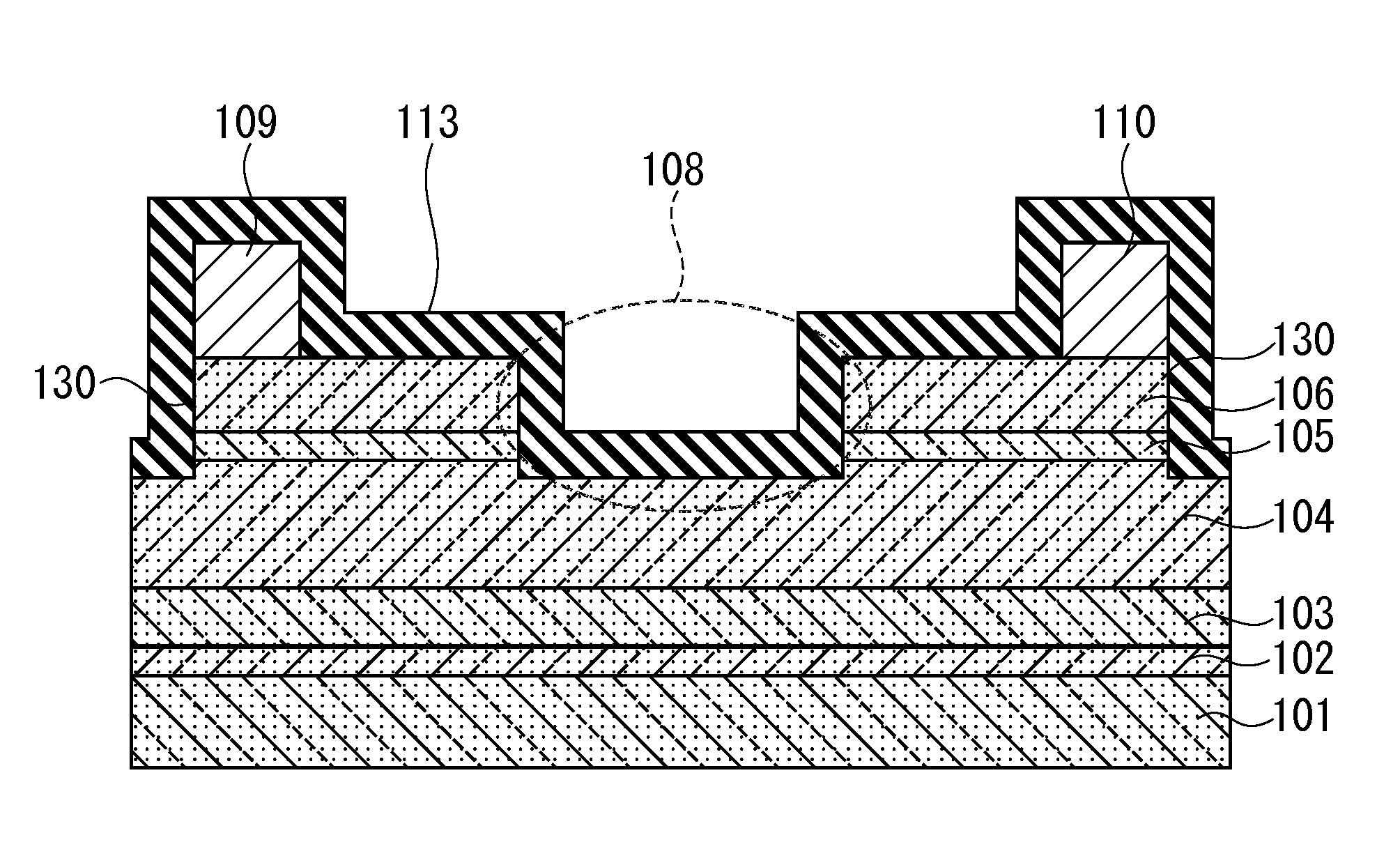
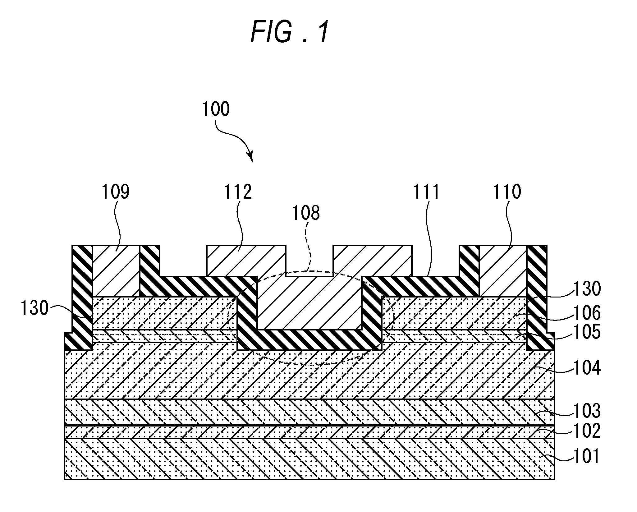
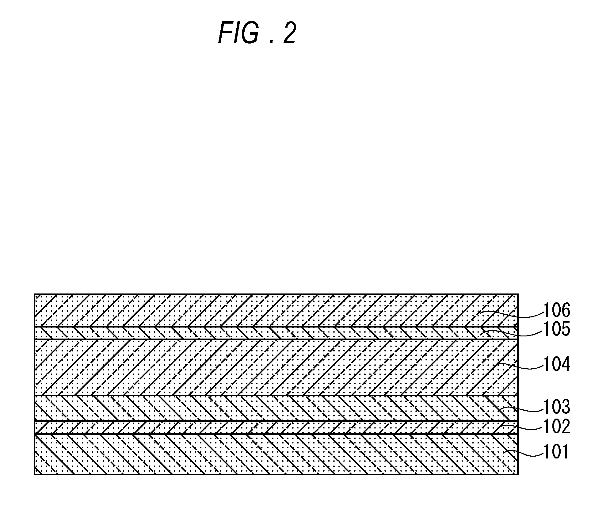
[0024]Here, FIG. 1 is a cross sectional view for exemplary showing a GaN-based field effect transistor (hereinafter refer to as an MOSFET) that is to be manufactured by making use of a method of manufacturing regarding one embodiment in accordance with the present invention. And then in accordance with such an MOSFET (100) there are designed to be performed a formation of an AlN layer (102) on to a substrate (101) that is to be comprised of such as a sapphire or an SiC or Si or the like, of a buffer layer (103) that is to be formed by performing a lamination of a GaN layer and an AlN layer as alternately thereon, and then of a channel layer (104) that is to be formed of a p-GaN thereon, respectively. Moreover, there are designed to be performed a lamination of a drift layer (105) that is to be formed of an undoped GaN (un-GaN) and then of an electron supplying layer (106) that has a band gap energy to be as larger with comparing to that of the drift layer (105) o...


PUM


Abstract

A method of manufacturing a GaN-based field effect transistor is provided by which a lower resistance and a higher breakdown voltage are obtained and which is less affected by a current collapse. A method of manufacturing the GaN-based field effect transistor(s) can comprise performing an epitaxial growth of an AlN layer (102), of a buffer layer (103), of a channel layer (104), of a drift layer (105) and of an electron supplying layer (106) in such the order on to a substrate (101) respectively; forming a recess part (108) thereon; performing an alloying process for performing an annealing in order to obtain an ohmic contact; forming a passivation layer (113) at a period of performing the annealing in the alloying process in order to protect the electron supplying layer (106) on to a surface of the recess part (108), on to the electron supplying layer (106), on to a source electrode (109) and on to a drain electrode (110), respectively; removing the passivation layer (113); forming a gate insulating film on to a surface at the inner side of the recess part (108), on to the electron supplying layer (106), on to the source electrode (109) and on to the drain electrode (110), respectively; and forming a gate electrode on to the gate insulating film at a part of the recess part (108).

Description

CROSS-REFERENCE TO RELATED APPLICATIONS[0001]This application claims priority from Japanese patent application serial No. 2009-034725, filed on Feb. 18, 2009, the entire content of which is incorporated herein by reference.BACKGROUND OF THE INVENTION[0002]1. Field of the Invention[0003]The present invention relate to a method of manufacturing a GaN-based field effect transistor that is formed of a nitride based compound semiconductor which is to be made use such as a device for a usage of a power electronics or a device for an amplification of high frequency or the like.[0004]2. Description of the Related Art[0005]A wide band gap semiconductor that is represented by a nitride based compound semiconductor of the III-V group has a high breakdown voltage, has an excellent property of an electronic transport, and has high heat conductivity. And then therefore the same is attractive as extremely for a material of a semiconductor device for a usage of such as a higher temperature, of a hi...

Claims


Application Information

Patent Timeline
Patent Type & Authority Patents(United States)
IPC IPC(8): H01L21/265
CPCH01L29/2003H01L29/78H01L29/66522
Inventor NOMURA, TAKEHIKOIKEDA, NARIAKIKAYA, SHUSUKEKATO, SADAHIRO
Owner FURUKAWA ELECTRIC CO LTD
Why Eureka
Try Eureka