Surface treatment method for germanium based device

a technology of germanium based devices and surface treatment methods, which is applied in the direction of cleaning using liquids, other chemical processes, semiconductor/solid-state device details, etc., can solve the problems of difficult to improve the performance of conventional si devices at a speed as before, the device performance is still not very ideal, and the problem of a lot of problems to be solved, etc., to achieve the effect of reducing the influence of the interface state, and easy formation

Inactive Publication Date: 2012-10-18
PEKING UNIV
View PDF3 Cites 2 Cited by
  • Summary
  • Abstract
  • Description
  • Claims
  • Application Information

AI Technical Summary

Benefits of technology

[0004]In order to solve the above-mentioned problems, the present invention provides a passivant for a surface of a germanium based device and a method for performing surface pretreatment to a germanium based device by using the passivant. The method is advantageous to improve the performance of the fabricated device, the process is simple, the cost is low, and the effect is significant. By performing surface pretreatment to a germanium based device using the passivant, the interface state may be reduced and the regeneration of natural oxidation layer and the out-diffusion of the germanium based substrate material can be effectively inhibited. The thermal stability of the metal germanide may also be improved significantly.
[0016]Firstly, through performing surface pretreatment to the germanium based device by using the aqueous solution of ammonium fluoride, fluorine with high electronegativity may be introduced onto the surface of the germanium based device, and stable Ge—F bonds are easily formed. Therefore, the surface pretreatment by the ammonium fluoride may passivate the germanium surface and reduce the influence of interface state. Secondly, during the film deposition and the annealing, the surface of germanium based device that has been subjected to the pretreament by the ammonium fluoride may be prevented from generating and volatileness of germanium monoxide gas and the out-diffusion of germanium is obviously reduced, so that a smooth and uniform surface is obtained. Thirdly, since the out-diffusion of germanium may be aggravated due to the presence of a natural oxidation layer so as to damage the surface of the germanium based device, it is necessary to remove the natural oxidation layer before the film deposition. However, once exposed to the atmosphere, the natural oxidation layer will be regenerated. The regeneration of the natural oxidation layer may be effectively inhibited by means of the ammonium fluoride pretreatment process, and the surface quality may be further improved. Fourthly, the ammonium fluoride pretreatment may also effectively inhibit the metal germanide from condensing and forming cavities under a higher annealing temperature, and significantly improve the thermal stability of the metal germanide. Fifthly, by means of the present method, the interface characteristics of the germanium based device are improved easily and effectively, the performance of the germanium based transistor is improved, and the surface passivation pretreatment is performed to the germanium based device without increasing the complexity of the process, which is very advantageous for process integration.

Problems solved by technology

However, with further shrinkage of the device feature size, the transistor gradually reaches both the physical limit and the technical limit, so that it is difficult to improve the performance of conventional Si device at a speed as before.
However, currently the fabrication technology of a germanium based device has not been fully developed, the performance of the device is still not very ideal and there are still a lot of problems to be solved.
Firstly, the interface of a germanium based device presents an interface state with relatively high density and the scattering is increased, which result in the degraded mobility of the germanium based device.
Secondly, at a relatively low temperature (330° C.
), an out-diffusion phenomenon may occur in a germanium based substrate material, that is, germanium diffuses toward outside of the substrate in the form of germanium monoxide gas, which results in that the morphology of the surface of the germanium based substrate and the film deposited thereon becomes worse and lead to increased current leakage.
Thirdly, the thermal stability of the metal germanide film is relatively poor, and the metal germanide film may be condensed to form a lot of cavities in the metal germanide film due to a nucleation and condensation reaction so that the property of the film becomes worse.
Above problems adversely affect the characteristics of the germanium based device and cause difficulties to the fabrication process of the germanium based device.

Method used


Image

  • Surface treatment method for germanium based device
  • Surface treatment method for germanium based device
  • Surface treatment method for germanium based device

Examples


Embodiment Construction

[0020]Hereinafter, the beneficial effects of performing surface pretreatment to a germanium based device by using an ammonium fluoride solution as a passivant are illustrated with reference to the accompanying drawings and a specific embodiment.

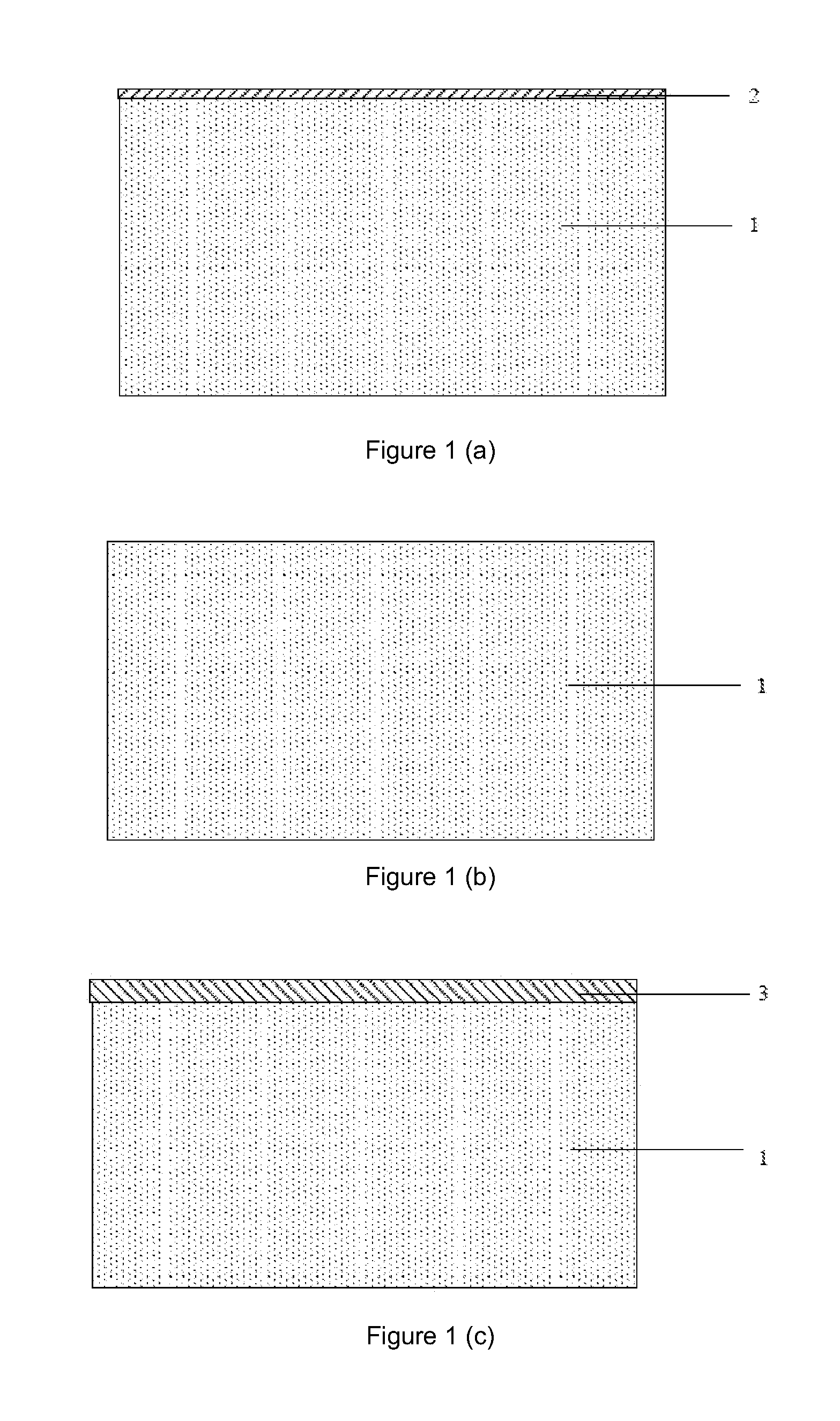
[0021]FIG. 1 is a flow chart illustrating a method of a specific embodiment for performing surface pretreatment to a germanium based device by using an ammonium fluoride solution as a passivant. The present embodiment comprises the following steps.

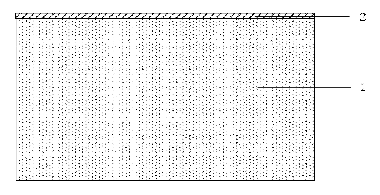
[0022]Step 1: a germanium based substrate is provided. As shown in FIG. 1(a), a semiconductor germanium substrate 1 is provided, wherein the semiconductor germanium substrate 1 may be a bulk germanium substrate, an epitaxial germanium substrate or a germanium on insulator (GOI) substrate, etc. The substrate may be P type doped or N type doped. On the surface of the semiconductor substrate 1, there may be a natural oxidation layer 2 which has a thickness of about 1 nm.

[0023]Step 2: a cleaning process...


PUM

PropertyMeasurementUnit
temperatureaaaaaaaaaa
thicknessaaaaaaaaaa
thicknessaaaaaaaaaa

Abstract

The present invention provides a surface treatment method for germanium based device. Through performing surface pretreatment to the germanium based device by using an aqueous solution of ammonium fluoride as a passivant, the interface state may be reduced, the formation of natural oxidation layer at the germanium surface may be inhibited, the regeneration of natural oxidation layer and the out-diffusion of the germanium based substrate material can be effectively inhibited, and the thermal stability of the metal germanide may also be increased significantly, so that the interface quality of the germanium based device is improved easily and effectively, which are advantageous to improve the performance of the germanium based transistor.

Description

FIELD OF THE INVENTION[0001]The present invention relates to the field of ultra large scale integrated circuit (ULSI) fabrication technology, in particular to a surface treatment method for a germanium based device.BACKGROUND OF THE INVENTION[0002]The integrated circuit technology has followed the Moore's law for over 40 years, and results in the rapid improvement of integrate circuit in the integration degree and performance, the reduction in the dimensional size of a metal-oxide-semiconductor field effect transistor (MOSFET) is a major means to improve operation speed and reduce production cost. However, with further shrinkage of the device feature size, the transistor gradually reaches both the physical limit and the technical limit, so that it is difficult to improve the performance of conventional Si device at a speed as before. Introduction of channel material with high mobility may further improve the device performance, thus currently, a germanium based device has become a h...

Claims


Application Information

Patent Timeline
Patent Type & Authority Applications(United States)
IPC IPC(8): C23G1/02C09K15/02H01L21/31B08B3/08
CPCC23C22/34C23C22/73H01L2924/0002H01L21/02052H01L21/02057H01L21/306H01L29/16H01L21/28255H01L21/28512H01L23/291H01L23/3171H01L29/45H01L21/28518H01L2924/00
Inventor AN, XIAGUO, YUEWANG, RUNSHENGHUANG, RUZHANG, XING
Owner PEKING UNIV
Why Eureka
Try Eureka