Method for manufacturing silicon carbide semiconductor device

a technology of silicon carbide and semiconductor devices, applied in the direction of semiconductor devices, electrical appliances, basic electric elements, etc., can solve the problems of increasing loss, achieve the effect of reducing the interface state and achieving high mobility

Active Publication Date: 2014-06-17
MITSUBISHI ELECTRIC CORP
View PDF7 Cites 2 Cited by
  • Summary
  • Abstract
  • Description
  • Claims
  • Application Information

AI Technical Summary

Benefits of technology

[0016]According to this invention, a silicon carbide field effect semiconductor device having sufficiently decreased interface state in the interface between a silicon carbide layer and a gate insulating film and having a carrier of high mobility of can be obtained.

Problems solved by technology

In some cases, the interface state decreases field effect mobility of MOSFET than mobility in a silicon carbide bulk, and increases resistance value of MOSFET in an on-operation state, thereby increasing loss.

Method used


Image

  • Method for manufacturing silicon carbide semiconductor device
  • Method for manufacturing silicon carbide semiconductor device
  • Method for manufacturing silicon carbide semiconductor device

Examples


embodiment 1

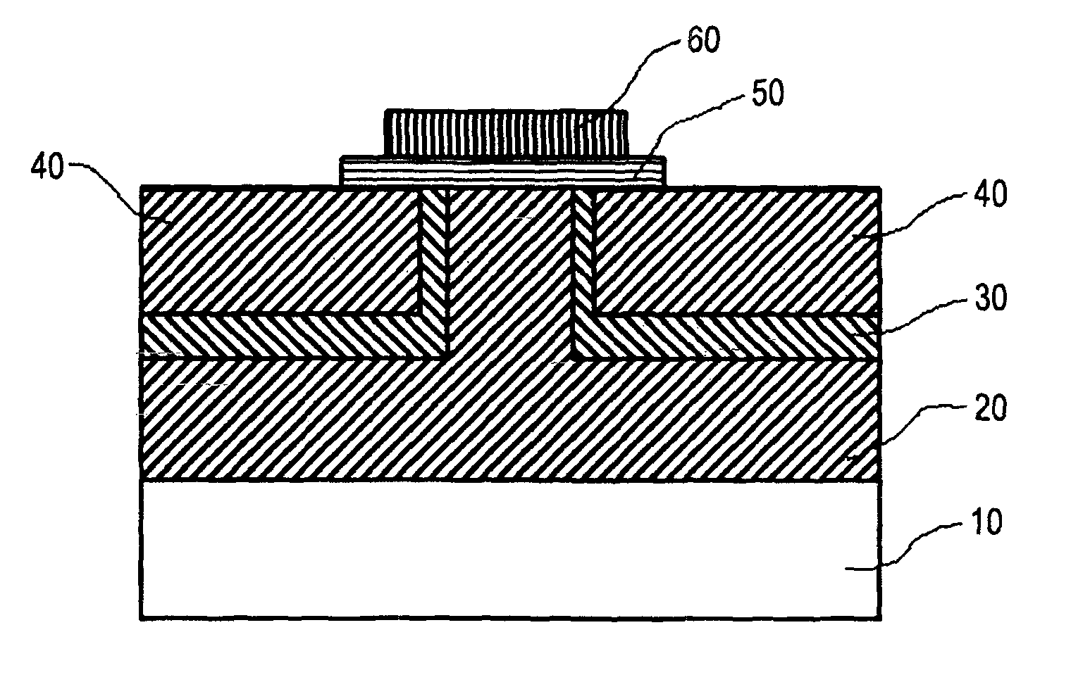
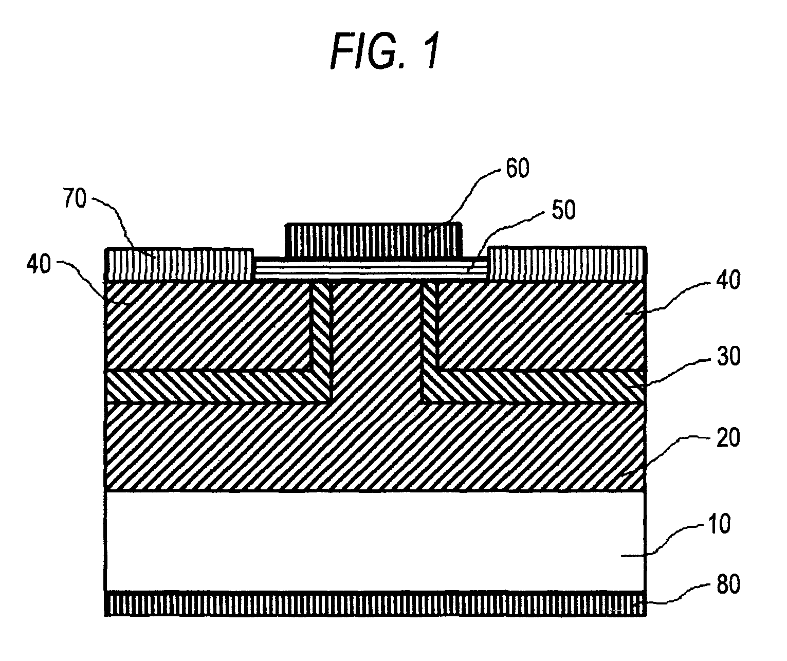
[0029]A cross-sectional schematic view of an element structure of-a silicon carbide semiconductor device produced by a method for manufacturing a silicon carbide semiconductor device of an embodiment 1 of the present invention is shown in FIG. 1. A cross-sectional structure of n-channel silicon carbide MOSFET is shown as one example of the-silicon carbide semiconductor device. In the present embodiment, a first conductive type is described as n-type, and a second conductive type is described as p-type.

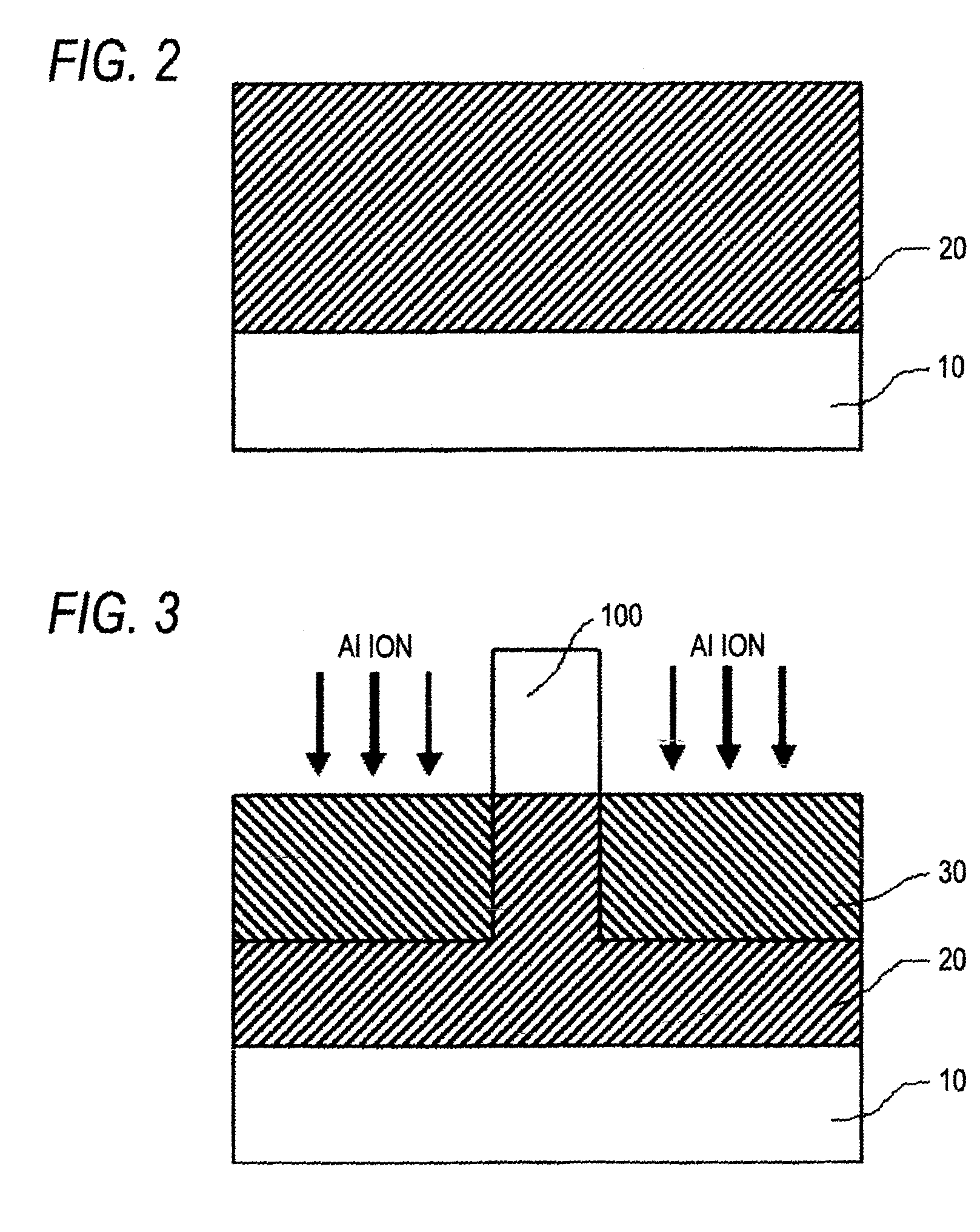
[0030]In FIG. 1, an n-type silicon carbide drift layer 20 is formed on a first principal surface of an n-type low resistance silicon carbide substrate 10. A p-type base region 30 containing aluminum (Al), which is a first impurity, as a p-type impurity is formed on a site separated with a certain width at a surface side of the silicon carbide drift layer 20. Furthermore, an n-type source region 40 containing nitrogen (N), which is a second impurity, as an n-type impurity is formed on a...


PUM

PropertyMeasurementUnit
retention timeaaaaaaaaaa
inner diameteraaaaaaaaaa

Abstract

In a silicon carbide MOSFET, interface state generated at an interface between a silicon carbide layer and a gate insulating film cannot be reduced sufficiently, and mobility of a carrier is decreased. To solve this problem, a silicon carbide semiconductor device according to this invention includes a substrate introduction step of introducing a substrate, which includes a silicon carbide layer on which a gate insulating film is formed, in a furnace, such that the substrate is arranged in a predetermined position of the furnace, and a heating step of heating the furnace having the substrate introduced therein while introducing nitrogen monoxide and nitrogen therein, wherein, in the heating step, nitrogen is reacted to nitride an interface between the gate insulating film and the silicon carbide layer.

Description

TECHNICAL FIELD[0001]This invention relates to a method for manufacturing a silicon carbide vertical field effect transistor which is a silicon carbide semiconductor device, and more particularly to a method for manufacturing a silicon carbide vertical field effect transistor for large electric power, having decreased on-resistance.BACKGROUND ART[0002]Silicon carbide has excellent physical values. Therefore, by utilizing its characteristic, it is expected to apply the silicon carbide to a power device having high pressure resistance and low loss.[0003]In the case of applying silicon carbide to a silicon carbide vertical metal-oxide film-semiconductor field effect transistor (Metal Oxide Semiconductor Field Effect Transistor: MOSFET) which is one kind of a silicon carbide semiconductor device, a gate insulating film such as a silicon dioxide layer is formed on the silicon carbide.[0004]In the case of forming the silicon dioxide film on the silicon carbide, a method of thermally oxidi...

Claims


Application Information

Patent Timeline
Patent Type & Authority Patents(United States)
IPC IPC(8): H01L21/20
CPCH01L21/3143H01L29/1608H01L21/02332H01L29/7802H01L21/0465H01L29/7827H01L29/66068H01L29/518H01L21/049
Inventor TANIOKA, TOSHIKAZUFURUHASHI, MASAYUKIIMAIZUMI, MASAYUKI
Owner MITSUBISHI ELECTRIC CORP
Why Eureka
Try Eureka