T-gate forming method and metamorphic high electron mobility transistor fabricating method using the same

a high electron mobility, transistor technology, applied in the direction of semiconductor devices, basic electric elements, electrical appliances, etc., can solve the problems of reducing the device gain at a high frequency region, deteriorating the device performance, and reducing the current gain, so as to achieve stable formation, high electron mobility, and high speed operation

Inactive Publication Date: 2008-07-31
POSTECH ACAD IND FOUND
View PDF2 Cites 43 Cited by
  • Summary
  • Abstract
  • Description
  • Claims
  • Application Information

AI Technical Summary

Benefits of technology

[0009]It is, therefore, an object of the present invention to provide a method for forming a stable T-gate by reducing physical impact on a minute gate during a metal removal process.
[0010]Another object of the present invention is to provide a method for manufacturing a metamorphic high electron mobility transistor with high performance by using an epitaxial structure capable of reducing parasitic resistance of a device.
[0026]In accordance with the present invention, the minute gate can be stably formed by the metal removal method using the adhesion member. Further, it is possible to form the high electron mobility transistor capable of performing high speed operation by employing the epitaxial structure having the highly doped indium phosphide etching protective layer to reduce a parasitic resistance component.

Problems solved by technology

However, the shorter the gate length is, the smaller the gate cross-sectional area becomes and the larger the resistance of a gate conducting wire results, which causes reduction of the device gain at a high frequency region, and particularly, reduction of the current gain.
That is, if the gate length is reduced, there is a chance that a gate can tip over due to physical impact that can be caused in a metal removal process, thereby deteriorating the performance of the device.
On the other hand, for most cases, although the gate length could be successfully reduced, unless parasitic resistance due to the epitaxial structure of the device is reduced, devices with a good current gain cut-off frequency will have a poor maximum oscillation frequency and devices having a good maximum oscillation frequency will have a poor current gain cut-off frequency.

Method used


Image

  • T-gate forming method and metamorphic high electron mobility transistor fabricating method using the same
  • T-gate forming method and metamorphic high electron mobility transistor fabricating method using the same
  • T-gate forming method and metamorphic high electron mobility transistor fabricating method using the same

Examples


Embodiment Construction

[0035]In the following description of the embodiments, reference is made to the accompanying drawings that form a part hereof, and in which is shown by way of illustration specific embodiments in which the invention may be practiced. It is to be understood that other embodiments may be utilized and structural changes may be made without departing from the scope of the present invention.

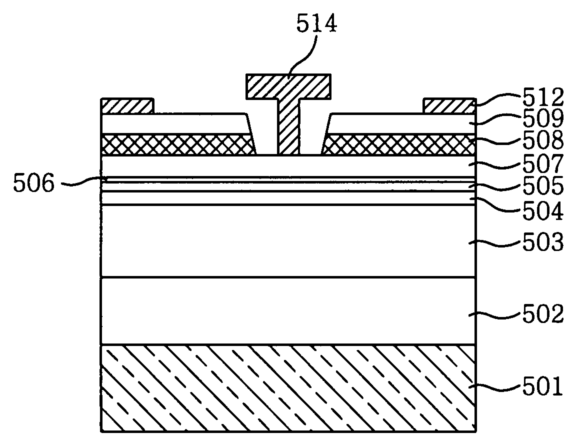
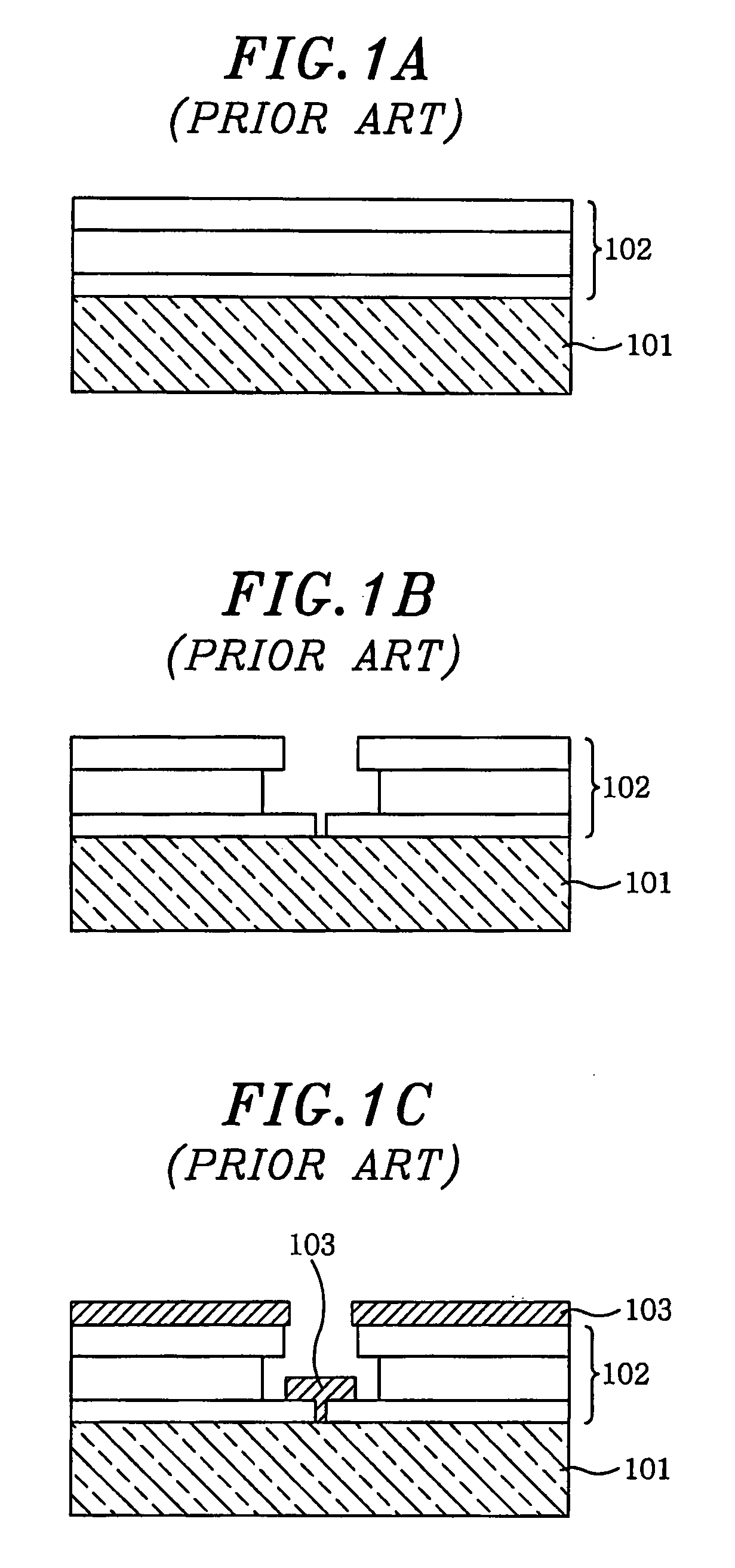
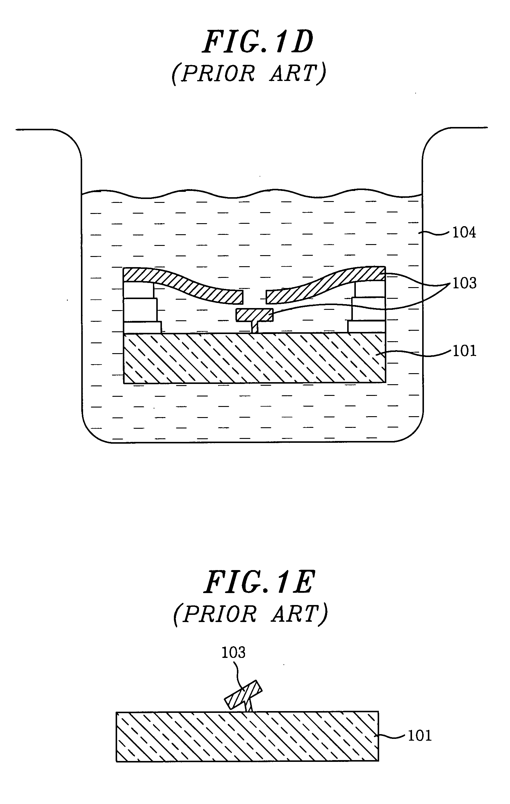
[0036]FIGS. 3A to 3F illustrate cross sectional views sequentially showing a process of forming a T-gate in accordance with the present invention. As shown in FIG. 3A, a plurality of resist films is sequentially laminated on a substrate 301. Herein, each laminated resist film has different sensitivity to the electron beam or reaction with a developing solution. For example, a bottom layer, i.e. a first resist film 302, is made of polymethyl methacrylate (PMMA) having relatively poor sensitivity to the electron beam, while a middle layer and a top layer, i.e. a second resist film 303 and a third resist...


PUM


Abstract

A method for forming a T-gate of a metamorphic high electron mobility transistor is provided. The method includes sequentially laminating a plurality of resist films on a substrate; forming a T-shaped pattern in the laminated resist films using electron beam lithography; forming a gate metal layer on the substrate where the T-shaped pattern has been formed; attaching an adhesion member to the gate metal layer formed on a top surface of the laminated resist films and detaching the adhesion member to thereby remove the gate metal layer; and removing the laminated resist films.

Description

FIELD OF THE INVENTION[0001]The present invention relates to a method for fabricating a metamorphic high electron mobility transistor (HEMT) that is based on a compound semiconductor; and, more particularly, it relates to a method for forming a stable T-gate on a substrate and optimizing an epitaxial structure to reduce parasitic resistance of a device.BACKGROUND OF THE INVENTION[0002]As communications technology has been developing around the world, communications devices applied to a higher frequency region of 2 GHz or more have been requiring higher electron mobility than the conventional devices. Therefore, compound semiconductors having high electron mobility such as gallium arsenide (GaAs), indium phosphide (InP) or the like are more widely used than silicon, which is typically used for more conventional devices. In a case where a field effect transistor is manufactured based on the compounds, the device characteristics thereof at an ultra-high frequency region, e.g., at a mil...

Claims


Application Information

Patent Timeline
Patent Type & Authority Applications(United States)
IPC IPC(8): H01L21/338
CPCH01L21/28587H01L29/7783H01L29/66462H01L29/42316H01L29/42376
Inventor JEONG, YOON-HALEE, KANG-SUNGKIM, YOUNG-SUHONG, YUN-KI
Owner POSTECH ACAD IND FOUND
Why Eureka
Try Eureka