Fabrication method of nitride-based semiconductor device

a technology of nitride and semiconductors, applied in the direction of semiconductor devices, basic electric elements, electrical appliances, etc., can solve the problems of low number of chips formed from one wafer, cracking, fracture, chipping, etc., and achieve the effect of preventing cracking, fracture, chipping

Active Publication Date: 2008-07-31
SHARP FUKUYAMA LASER CO LTD
View PDF39 Cites 22 Cited by
  • Summary
  • Abstract
  • Description
  • Claims
  • Application Information

AI Technical Summary

Benefits of technology

[0010]In view of the foregoing, an object of the present invention is to provide a fabrication method of a nitride-based semiconductor device th...

Problems solved by technology

However, this device structure is disadvantageous in that the electrodes occupy a relatively large area since two electrodes are formed on the nitride-based semiconductor layer, leading to the problem that the number of chips f...

Method used


Image

  • Fabrication method of nitride-based semiconductor device
  • Fabrication method of nitride-based semiconductor device
  • Fabrication method of nitride-based semiconductor device

Examples


example 1

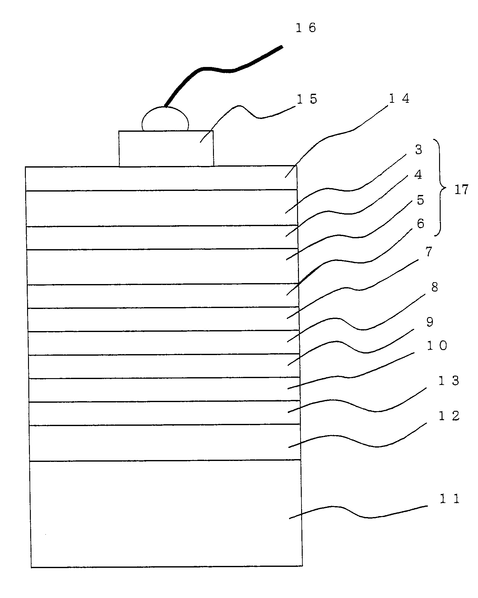
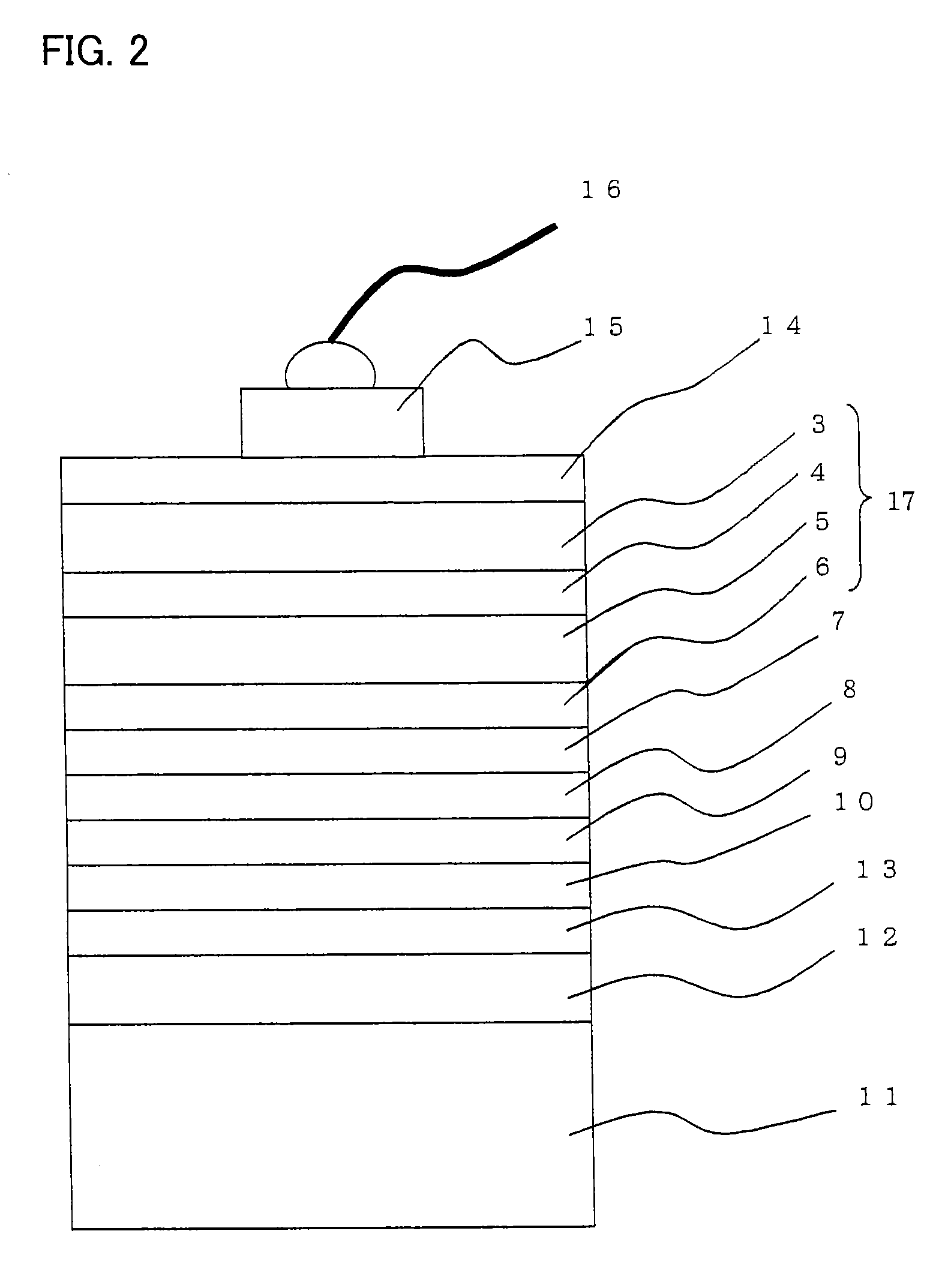
[0055]In the present example, a GaN based LED corresponding to a structure as shown in FIG. 2 was produced as a nitride-based semiconductor device by the stacked structure formation step, first bonding metal deposition step, second bonding metal deposition step, bonding step, mirror-polishing step, support substrate removal step, and the conventional well-known step.

[0056]

[0057]A C-plane sapphire wafer having a diameter of 50.2 mm and thickness of 430 μm was employed as support substrate 1. Support substrate I was placed in an MOCVD device, raised in temperature up to 1100° C. in a hydrogen ambient for thermal etching.

[0058]Next, the temperature was lowered down to 300° C., and trimethyl gallium (TMG) as the group III raw material and ammonia as the N raw material were fed to grow a low-temperature deposited GaN buffer layer having a thickness of 20 nm. Then, the temperature was raised to 1000° C., and trimethyl gallium (TMG), ammonia and SiH4 were fed as the raw material to grow Si...


PUM


Abstract

A fabrication method of a nitride-based semiconductor device includes the steps of forming a stacked structure constituted of a nitride-based semiconductor on a support substrate, depositing a first bonding metal on the stacked structure, depositing a second bonding metal on a retention substrate, bonding the first bonding metal and the second bonding metal in a state where the first bonding metal and the second bonding metal face each other to unite the retention substrate and the stacked structure, wherein the first bonding metal and the second bonding metal constitute the bonding metal, and separating the support substrate from the stacked structure for removal. The area of the surface of the retention substrate is set smaller than the area of the surface of the support substrate. Accordingly, cracking, fracture, chipping, and the like at the retention substrate can be prevented.

Description

[0001]This nonprovisional application is based on Japanese Patent Application No. 2006-297329 filed with the Japan Patent Office on Nov. 1, 2006, the entire contents of which are hereby incorporated by reference.BACKGROUND OF THE INVENTION[0002]1. Field of the Invention[0003]The present invention relates to a fabrication method of a nitride-based semiconductor device, particularly a fabrication method of a nitride-based semiconductor device, removing a support substrate on which a nitride-based semiconductor layer is formed after bonding between the nitride-based semiconductor layer and a retention substrate.[0004]2. Description of the Background Art[0005]A nitride-based semiconductor device typically employs a nitride-based compound semiconductor for the major portion of the device structure. Various devices such as a light emitting device, a light receiving device and a power device can be enumerated. In the case of a light emitting device such as an LED (Light Emitting Diode) or ...

Claims


Application Information

Patent Timeline
IPC IPC(8): H01L21/30H01L33/42H01L33/32
CPCH01L33/0079H01L33/0093
Inventor HATA, TOSHIO
Owner SHARP FUKUYAMA LASER CO LTD
Why Eureka
Try Eureka