Thermal interface for electronic chip testing

a technology of electronic chips and thermal interfaces, applied in individual semiconductor device testing, semiconductor/solid-state device testing/measurement, instruments, etc., can solve the problems of increasing power consumption and associated heat generation in these devices, becoming a considerable challenge to manage this thermal load, and it is difficult to meet all of these requirements using existing thermal interface materials

Inactive Publication Date: 2008-08-14
APPLE INC
View PDF10 Cites 50 Cited by
  • Summary
  • Abstract
  • Description
  • Claims
  • Application Information

AI Technical Summary

Benefits of technology

[0010]In some embodiments, the heat-removal device is coated with a layer that facilitates wetting with the thermal interface. For example, the layer may include a metal, such as gold, platinum, tantalum, titanium, tin, chromium, nickel, zinc, silver, and / or aluminum.
[0018]In some embodiments, the method additionally involves applying the thermal interface to the second surface of the second semiconductor die. Then, the second semiconductor die is positioned in the test apparatus such that the first surface of the second semiconductor die is coupled to the connector and the thermal interface is coupled to the heat-removal device, thereby facilitating simultaneous testing of the first semiconductor die and the second semiconductor die.

Problems solved by technology

This has resulted in significantly increased power consumption and associated heat generation in these devices.
Consequently, it is becoming a considerable challenge to manage this thermal load to maintain acceptable internal and external operating temperatures in these ICs.
This problem is particularly acute during testing of bare semiconductor dies (at the wafer, die, or chip level) that are to be used in ICs, since these semiconductor dies are not yet packaged.
Unfortunately, it is difficult meet all of these requirements using existing thermal interface materials.
For example while existing thermally conductive materials (such as silicone-based grease or propylene glycol) have a moderate thermal conductivity, the thermal impedance associated with these thermal interface materials often limits the heat removal from the die.
This has made it difficult to test semiconductor dies at maximum power or maximum operating temperatures, especially as the thermal load generated by successive generations of semiconductor dies has increased.
Furthermore, silicone-based thermal greases often leave residue on the semiconductor die.

Method used


Image

  • Thermal interface for electronic chip testing
  • Thermal interface for electronic chip testing
  • Thermal interface for electronic chip testing

Examples


Embodiment Construction

[0029]The following description is presented to enable any person skilled in the art to make and use the invention, and is provided in the context of a particular application and its requirements. Various modifications to the disclosed embodiments will be readily apparent to those skilled in the art, and the general principles defined herein may be applied to other embodiments and applications without departing from the spirit and scope of the present invention. Thus, the present invention is not intended to be limited to the embodiments shown, but is to be accorded the widest scope consistent with the principles and features disclosed herein.

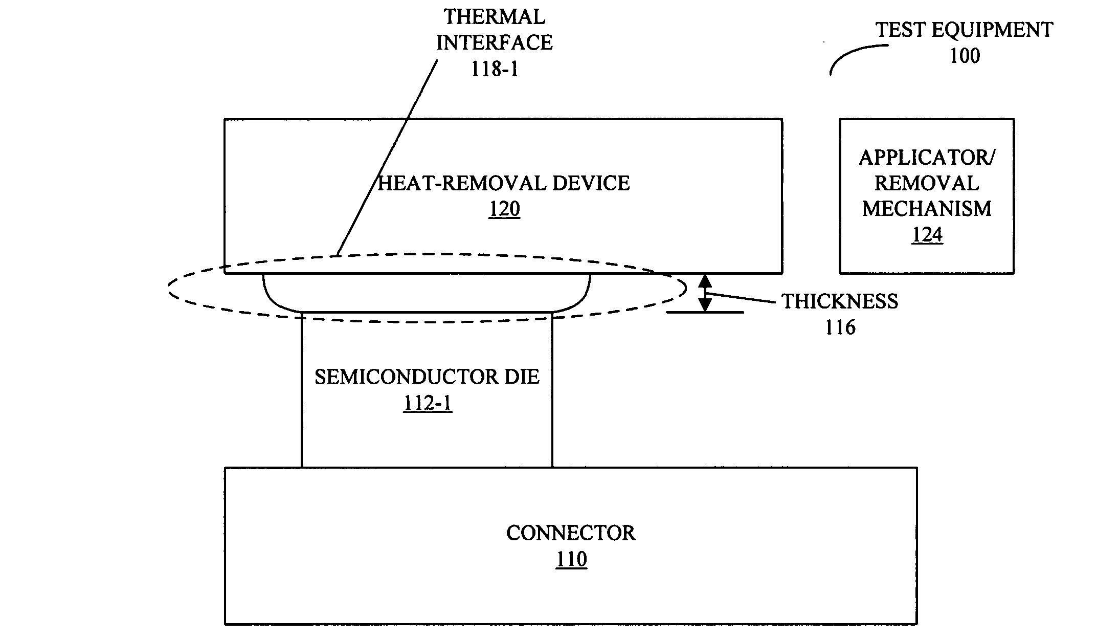
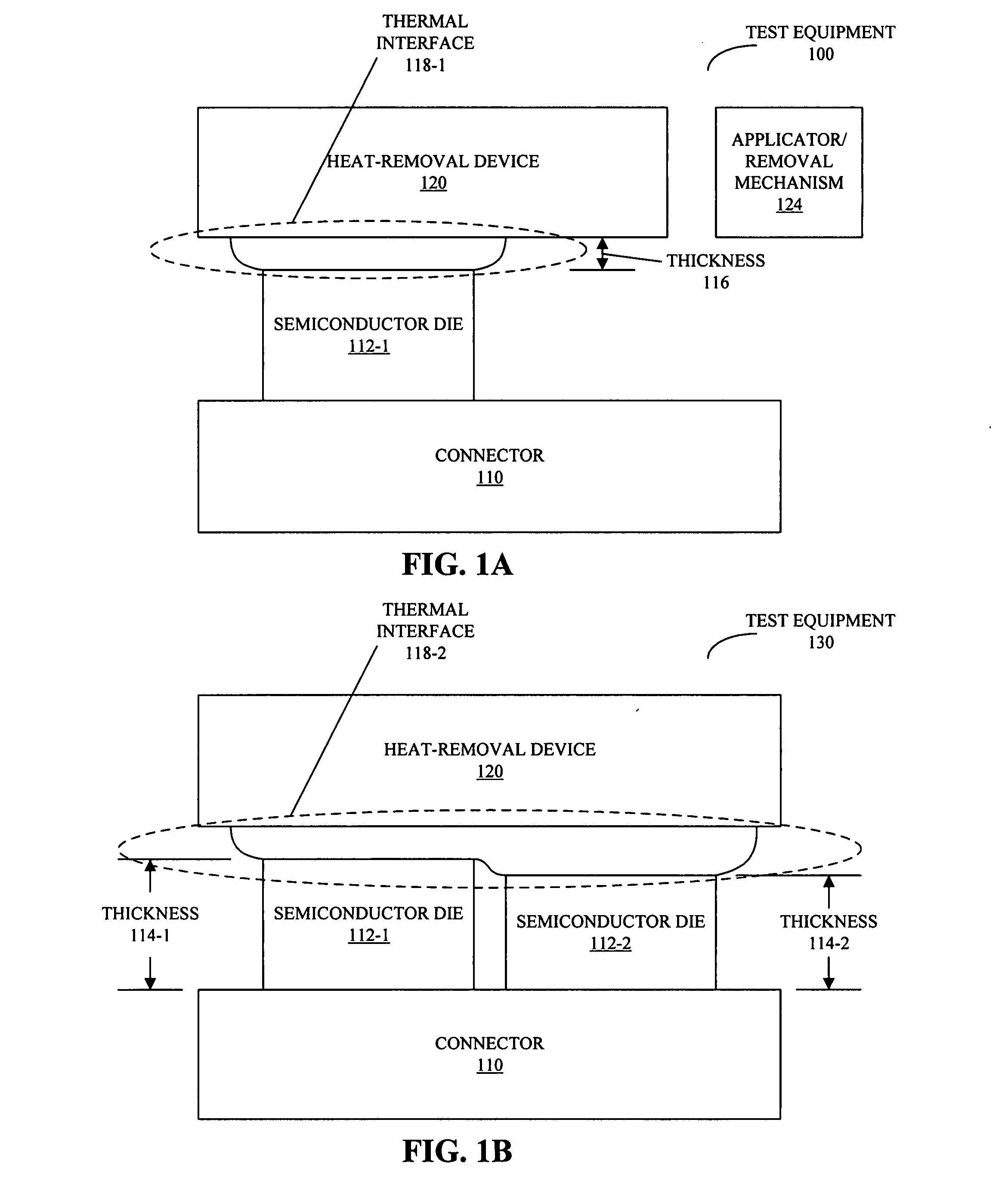
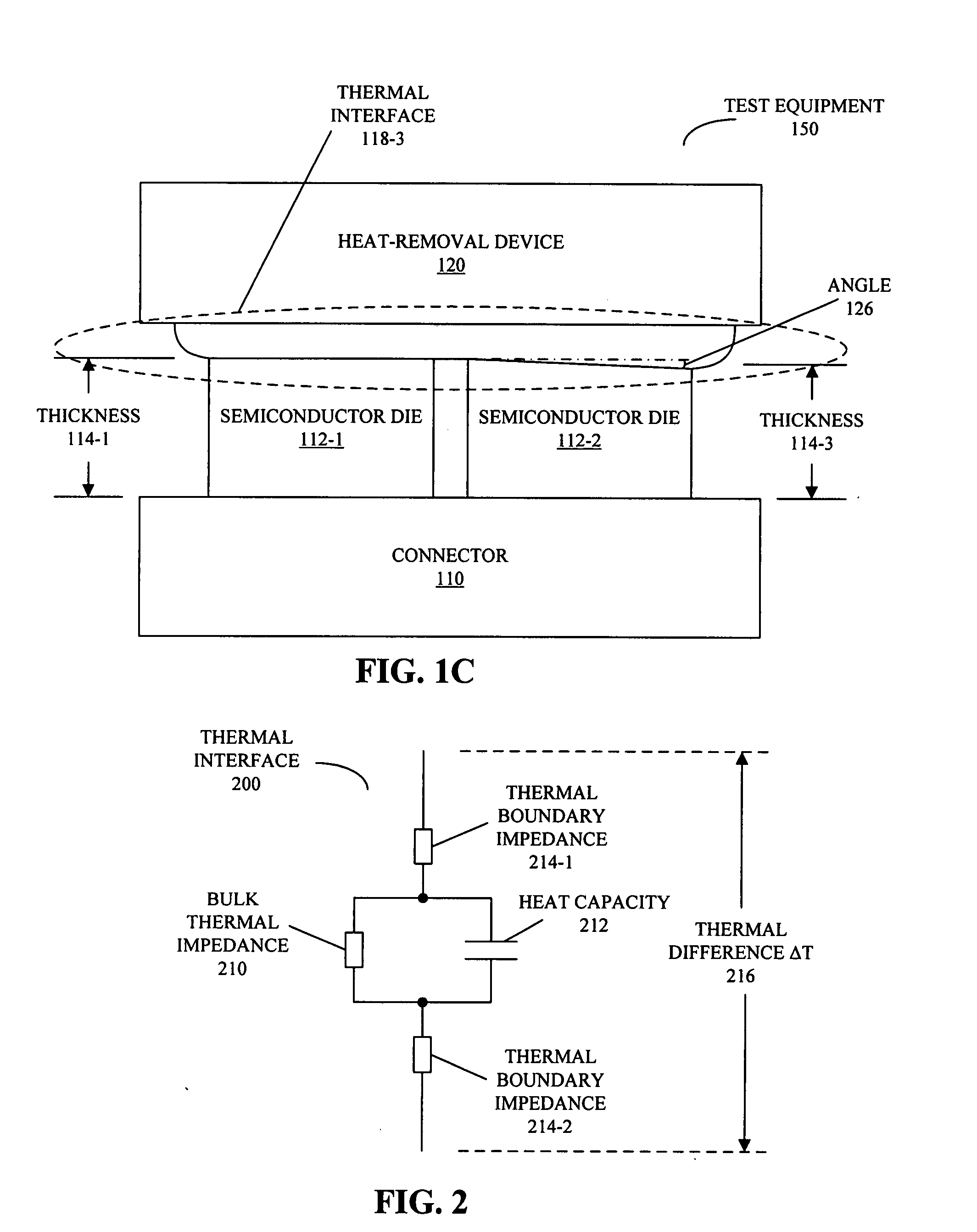
[0030]Embodiments of an apparatus and a technique for performing electrical testing (such as functional testing, frequency testing, burn-in testing, and / or accelerated life testing) of a semiconductor die or chip are described. In particular, the apparatus, which may include automated test equipment (ATE) and / or semiconductor-die burn-in equipm...


PUM


Abstract

An apparatus that performs electrical testing is described. This apparatus includes a first semiconductor die that is to be tested, and a connector configured to be coupled to a first surface of the first semiconductor die. Furthermore, a thermal interface in the apparatus is between a second surface of the first semiconductor die and a heat-removal device. This thermal interface includes a metal which is in a liquid state at an operating temperature of the semiconductor die during the testing.

Description

BACKGROUND[0001]1. Field of the Invention[0002]The present invention relates to heat-transfer techniques. More specifically, the present invention relates to test equipment that includes a low melting-point metal alloy which functions as a thermal interface during testing of electronic components.[0003]2. Related Art[0004]The functionality, performance, and operating speed of integrated circuits (ICs) have increased significantly in recent years. This has resulted in significantly increased power consumption and associated heat generation in these devices. Consequently, it is becoming a considerable challenge to manage this thermal load to maintain acceptable internal and external operating temperatures in these ICs. This problem is particularly acute during testing of bare semiconductor dies (at the wafer, die, or chip level) that are to be used in ICs, since these semiconductor dies are not yet packaged.[0005]Proper thermal coupling to the semiconductor dies during testing is need...

Claims


Application Information

Patent Timeline
Patent Type & Authority Applications(United States)
IPC IPC(8): H01L21/66G01R31/26
CPCG01R31/2874
Inventor BLANCO, RICHARD LIDIOHILLMAN, MICHAEL D.
Owner APPLE INC
Why Eureka
Try Eureka