

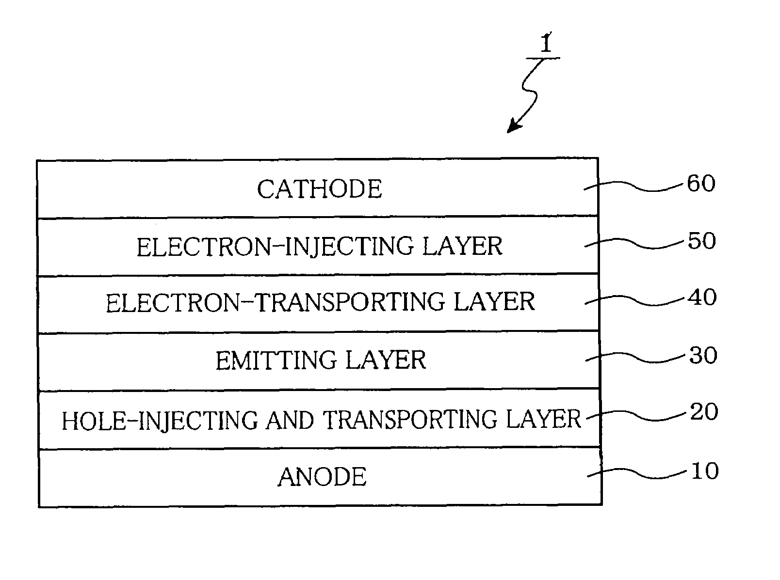
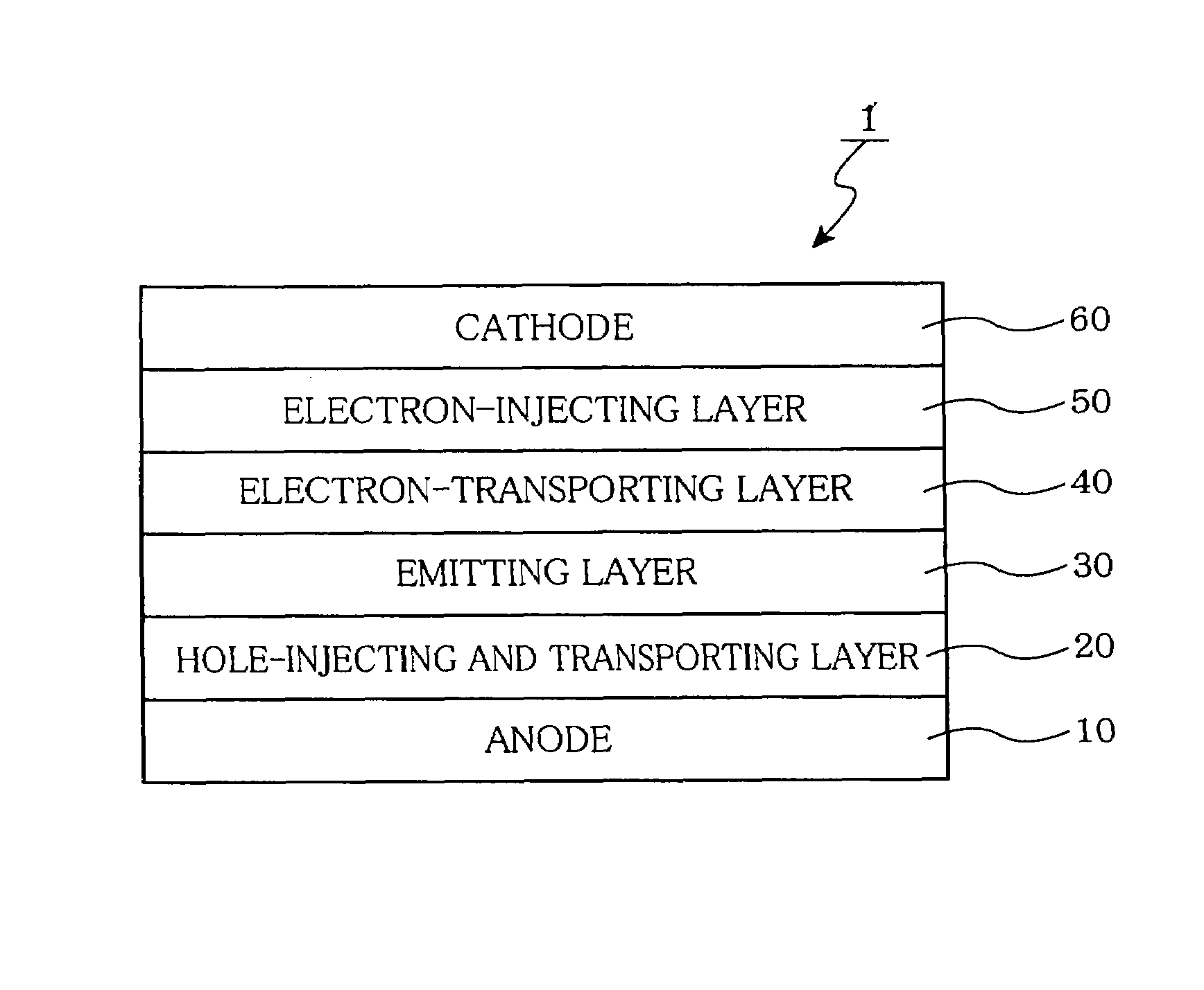
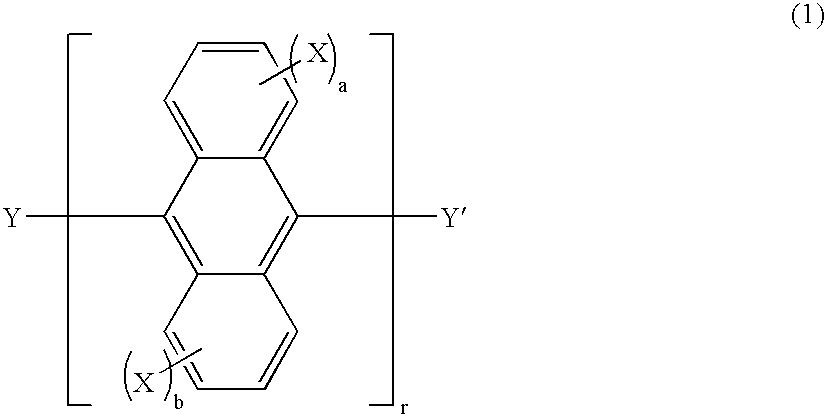
Organic electroluminescent device
- Summary
- Abstract
- Description
- Claims
- Application Information
AI Technical Summary
Benefits of technology
Problems solved by technology
Method used
Image

Examples
example 1
[0192]A glass substrate of 25 mm by 75 mm by 1.1 mm thick with an ITO transparent electrode (film thickness: 130 nm) (GEOMATEC Co., Ltd.) was subjected to ultrasonic cleaning with isopropyl alcohol for 5 minutes, followed by ultrasonic cleaning with distilled water having an electric resistance of 20 MΩm for 5 minutes. The ITO substrate was further subjected to ultrasonic cleaning with isopropyl alcohol for 5 minutes. Thereafter, the ITO substrate was taken out and dried. Immediately after, the substrate was then subjected to UV-ozone cleaning for 30 minutes by means of an UV-ozone cleaning apparatus manufactured by SAMCO International, Inc.
[0193]The cleaned glass substrate with transparent electrode lines formed thereon was secured to a substrate holder of a vacuum deposition apparatus. The inside of the apparatus was vacuumed to 1×10⁻⁵ Pa. Subsequently, a 60 nm-thick N,N′-bis(N,N′-diphenyl-4-aminophenyl)-N,N-diphenyl-4,4′-diamino-1,1′-biphenyl (hereinafter abbreviated as the “TPD ...
examples 2 to 26
[0197]Organic EL devices were fabricated in the same manner as in Example 1, except that the materials shown in Table 2 were used as the material for the electron-transporting layer or the electron-injecting layer. The results of the evaluation of the device are shown in Table 2. The luminance half life of the device was the same as that of the device in Example 1.
PUM
| Property | Measurement | Unit |
|---|---|---|
| Fluorescence quantum yield | aaaaa | aaaaa |
Abstract
Description
Claims
Application Information